Tutorial 0: Quickstart
examples/tutorials/00_quickstart_klive_and_pdk.ipynb builds a one-qubit chip from nothing, one component per cell:
two pads, a feedline, an Xmon with a trilayer junction and a λ/4 hanger readout. After every step it shows the
layout, the DRC, the netlist and the LOM. It ends with the FEM round trip, a feedback step and the fab export. Start
here: tutorials 1 to 4 repeat the same steps on bigger chips.
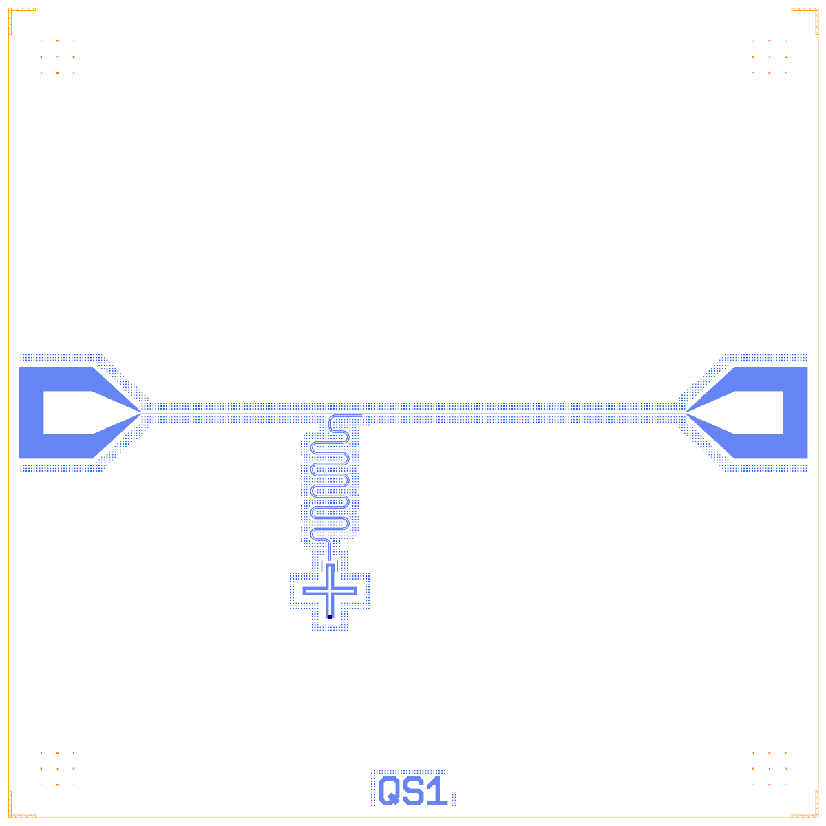
The finished chip (section 6): two pads, the feedline, the Xmon and its meandered λ/4 readout.
The sections
Section |
What it does |
Call |
What comes out |
|---|---|---|---|
1 PDK |
Reads the process design kit every build uses |
|
A table of the stack, the CPW, the die frame and the pad, junction and keep-out rules, then the fab layer map |
2 Die and live view |
Starts an empty 7.5 × 7.5 mm die |
|
An empty die with the QCT frame |
3 Pads |
Two bond pads at the 100 µm rule |
|
Pads slid to 100 µm from the die edge; DRC with 2 |
4 Feedline |
One CPW between the pads |
|
DRC clean; a netlist with nodes |
5 Qubit |
An Xmon with one claw and a trilayer junction sized from a target |
|
C_Σ ≈ 99.2 fF, L_J 6.92 nH, R_n 46.2 kΩ (inside 40 to 50 kΩ) |
6 Readout |
A λ/4 hanger from the claw to the feedline |
|
R1 of 4501 µm; DRC clean |
7 Netlist and LOM |
Builds the netlist and simulates it |
|
Modes and a table of values against the targets |
8 Iterate |
Rescales the R1 length until f_r is within 0.2 % |
|
A before/after table |
9 FEM stage 1 |
One sim group, three jobs, and the subset check |
|
Convergence table, C-matrix, eigenmodes, S21 notch, FEM-filled capacitances |
10 FEM stage 2 |
The subset values in the whole LOM |
|
Three LOM-versus-FEM tables (Q3D, eigenmode, driven) |
11 Feedback |
One consensus and the next revision |
|
A table of proposed knobs and revision 1 (DRC clean) |
12 Fab export |
Cheese, rounding and the 3/0 keep-out |
|
A fab layer table and the qubit’s fab picture |
13 Snapshots |
The junction close up |
|
Two junction pictures |
14 Summary |
A table of the whole run |
The header cells also explain the loop (design, DRC, LOM, FEM, feedback) and the two FEM stages and their switches.
1 to 4: PDK, die, pads, feedline
The PDK is quantcore_nb_sapphire_v1: sapphire 650 µm, εr 10.25, Nb film, CPW 10/6 µm (about 50 Ω), a 100 µm pad
edge, Nb/AlOx/Nb trilayer junctions with R_n 40 to 50 kΩ, and a negative-mask fab layer map. See
the PDK page.
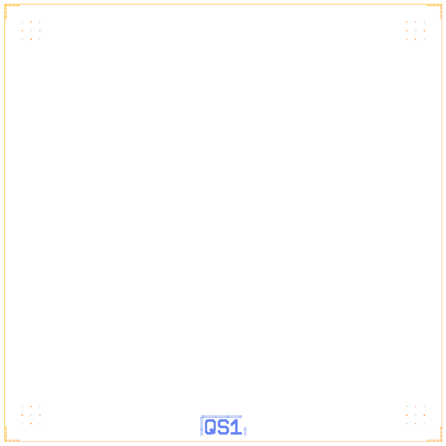
Section 2: the empty die with the PDK frame (dicing marks, alignment grids, device ID QS1).
edge="auto" is the 100 µm rule at work. The notebook asks for the pads at x = 1125 and x = 6375 µm and prints where
the ports end up: PAD_W.a at 1225 µm and PAD_E.a at 6275 µm. The pad slides until its outer etch edge is 100 µm
from the die edge. Without edge="auto" the DRC adds a pad_edge design warning.
5 and 6: the qubit and its readout
The Xmon has a 450 µm cross. A 300 µm cross would have needed R_n of about 66 kΩ for 5.5 GHz, outside the PDK window, so the capacitance sets the frequency here and the junction is sized from it.

Section 5: the Xmon with its claw (top) and the junction at the foot of the south arm.
The readout length starts from the bare λ/4 for 7.0 GHz (v_ph = 0.4204 c on the PDK stack). near=(x, y) centres the
coupler at the feedline point nearest to (x, y), so it stays put if the feedline start moves.
7 and 8: LOM and the first iteration
simulate(fill(model, design)) runs QuCat for the normal modes and κ, then QuTiP for the dressed values. With
component estimates only:
Quantity |
LOM |
Target |
|---|---|---|
Q1 f_q |
5.51 GHz |
5.5 GHz |
Q1 α |
-182.18 MHz |
|
R1 f_r |
6.2518 GHz |
7 GHz |
R1 χ |
-1.1288 MHz |
|
R1 κ |
0.13536 MHz |
The qubit lands on target. The resonator is 0.75 GHz low: the claw (about 80 fF at the open end) loads the λ/4. Section 8 scales the drawn length by f_r / target. It needs two steps: 4020 µm gives 6.9153 GHz, 3971 µm gives 6.9904 GHz, within 0.2 % of 7.0 GHz.
9 and 10: the FEM round trip
Q1R1 is the qubit and its readout with a 300 µm margin; here it is the whole chip minus the two pads. Each analysis
makes its own job in build/jobs/t00_quickstart_Q1R1_<analysis>/:
Analysis |
What the box holds |
Gives |
|---|---|---|
|
The qubit and a 100 µm stub of R1 (cut at the claw) |
The C-matrix: island, claw, C_g |
|
The qubit, R1, and the feedline cut into two 50 Ω ports |
Modes with f, Q, p_J; pyEPR f, α, χ |
|
The same box, driven |
The S21 notch of R1: f0, κ_ext |
The kept results (fast settings):
Job |
Passes |
Last Δ / target |
Converged |
Wall time |
|---|---|---|---|---|
Q3D |
7 |
1.94 / 2.0 % |
no |
41.6 s |
Eigenmode |
3 |
3.14 / 1.0 % |
no |
392.8 s |
Driven |
2 |
0.0476 / 0.05 |
yes |
167.3 s |
The C-matrix gives C_island 101.4 fF and C_g 2.943 fF. In stage 2 the same LOM is run on three sets of values:
Quantity |
LOM (estimates) |
LOM on Q3D |
Eigenmode + pyEPR |
Driven S21 fit |
|---|---|---|---|---|
Q1 f_q (GHz) |
5.511 |
5.462 (-0.9 %) |
5.157 (-6.4 %) |
|
Q1 α (MHz) |
-182.9 |
-179.5 (+1.8 %) |
-153.4 (+16.1 %) |
|
R1 f_r (GHz) |
6.99 |
7.086 (+1.4 %) |
6.855 (-1.9 %) |
6.698 (-4.2 %) |
R1 χ (MHz) |
-0.43 |
-0.3159 (+26.5 %) |
-0.1889 (+56.1 %) |
|
R1 κ (MHz) |
0.1873 |
0.1978 (+5.6 %) |
0.2886 (+54.1 %) |
0.3213 (+71.5 %) |
11: feedback
loop.analyse puts every result into one consensus: the C-matrix fills the circuit, the eigenmode adds the pyepr
estimator and the driven fit fills the hanger κ. loop.feedback then solves for knobs that put every target inside
its tolerance and writes build/t00/revisions/rev1.json. The proposed knobs:
Knob |
Now |
Proposed |
|---|---|---|
|
6.8719 |
6.064 |
|
3971.5 |
3880.7 |
The predicted effect is f_q 5.1565 to 5.4999 GHz and f_r 6.8554 to 7.0 GHz. The revision passes the DRC. Nothing is re-simulated in this notebook; tutorial 4 closes that loop.
12 to 14: fab export
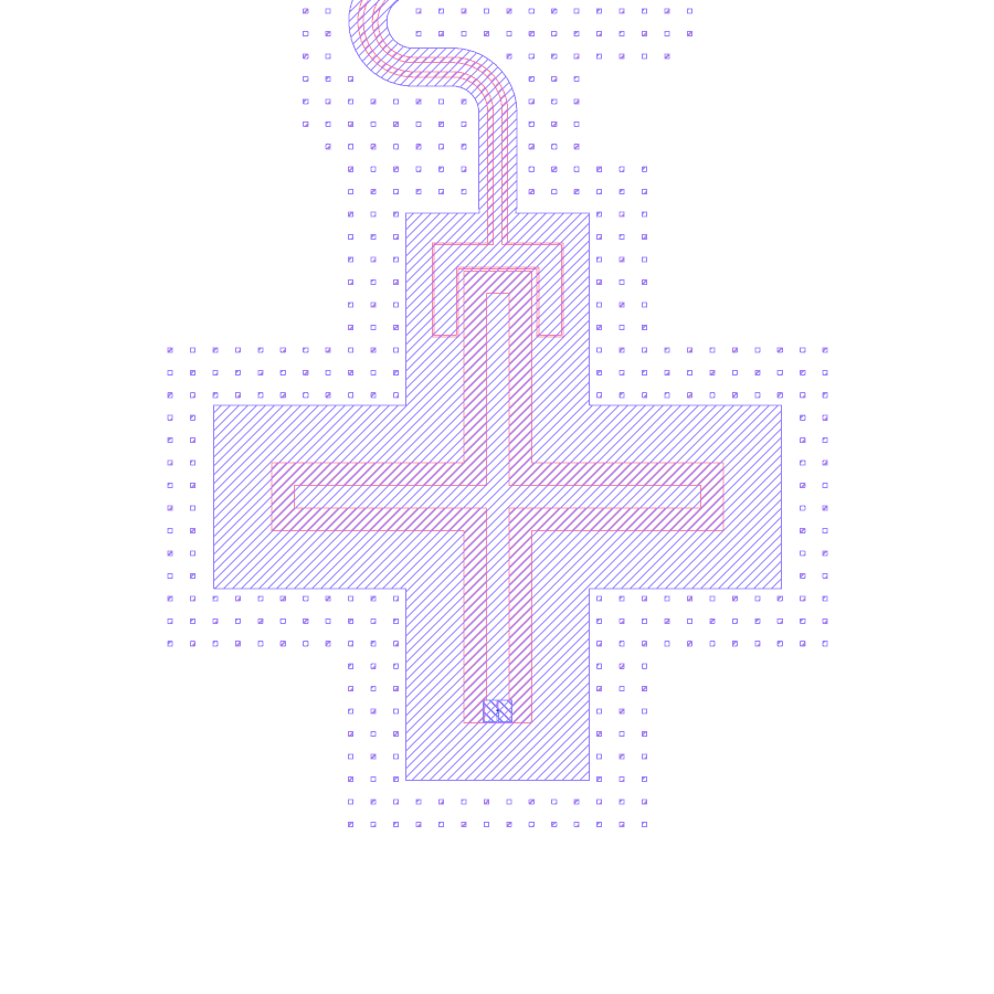
Section 12: the fab view of the qubit: etch, the 3/0 keep-out, the cheese band and rounded corners.
export_fab writes only the PDK fab layers (flat), keeps the cheese the build drew (2772 holes: the PDK band of 5 µm
squares around the 3/0 keep-outs) and rounds the corners. The report lists the polygons per fab layer (M1 2778,
M3 2776, JJ_STRAIGHT 1, JJ_BENT 1, MARKERS_ALIGN 36, MARKERS_DICING 4, and so on). The CLI does the same:
qcc mask examples/tutorials/designs/t00_quickstart.json (--no-cheese, --no-round switch the rules off). See
Fab.
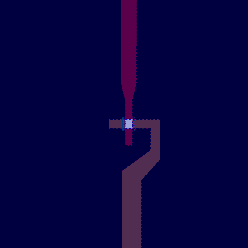
Section 13: the trilayer junction (finger overlap and spacer layers).
Pitfalls
The claw loads the resonator’s open end, so the bare λ/4 length is always too long. Iterate (section 8).
The FEM tables of section 9 are fast-setting results: the eigenmode job reached 3.14 % against a 1 % target. The qubit frequency spans 5.157 to 5.511 GHz across the three methods; the feedback step works from that spread, it is not a verdict on the design.
Every kept result prints the “solved for another revision” note. That is expected (see the index).
A DRC warning about a dangling port right after placing a component is normal: nothing is connected yet.
Tutorial 1 applies the same steps to a nine-qubit chip.