Six-resonator chip (chip_07)
A resonator test chip. One 10/6 µm feedline runs between two bond pads, and six λ/4 hanger resonators hang off it, three above and three below, each coupled along a short straight section. Every resonator has its own length, so it rings at its own frequency (targets 5.0 to 6.5 GHz, written on the chip as 50 to 65). Measuring the transmission through the feedline shows six dips, which give the resonator frequencies, coupling and quality factors before any qubit is added.
It comes from Quantcore’s own QWri script chip_07_resonators.py (May 2024, internal). The Quantcore-PDK rebuild puts the saved design in the PDK die frame and moves the bond pads to the 100 µm pad-edge rule, so the feedline is 5050 µm instead of 5250 µm. The PDK cheese (5 µm squares with 20 µm gaps, at least 4 µm from the 3/0 keep-outs) now covers the whole die, and the holes drawn in the original layout stay. Build it to see the simplest chip in this set: a feedline with resonators coupled by proximity.
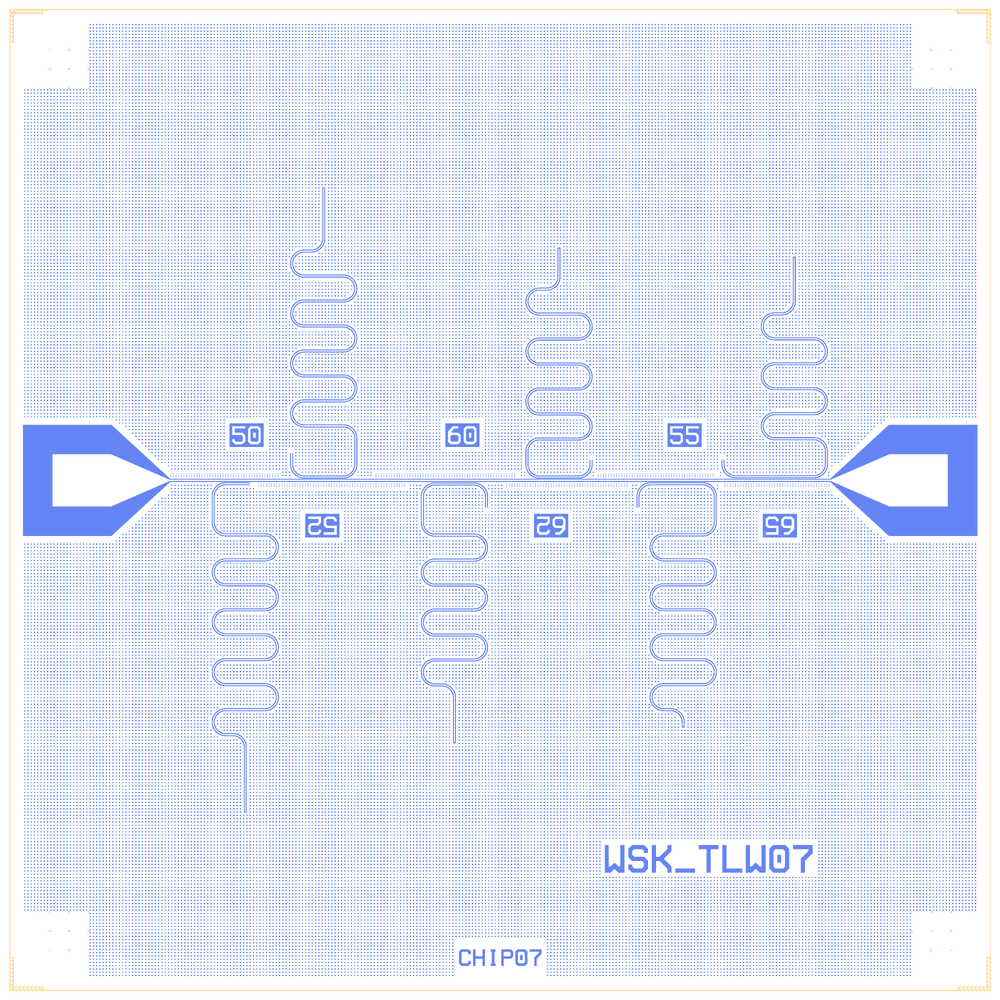
At a glance
Notebook |
|
Source |
Quantcore legacy QWri script |
Chip |
7.5 × 7.5 mm Quantcore die, sapphire, CPW 10 / 6 µm |
On the chip |
1 feedline between 2 bond pads · 6 λ/4 hanger resonators · 6 flux-hole arrays · labels |
Builds today |
yes, rebuilt from its JSON on 2026-11-19 in 2.2 s (the notebook itself was not re-run) |
Pictures
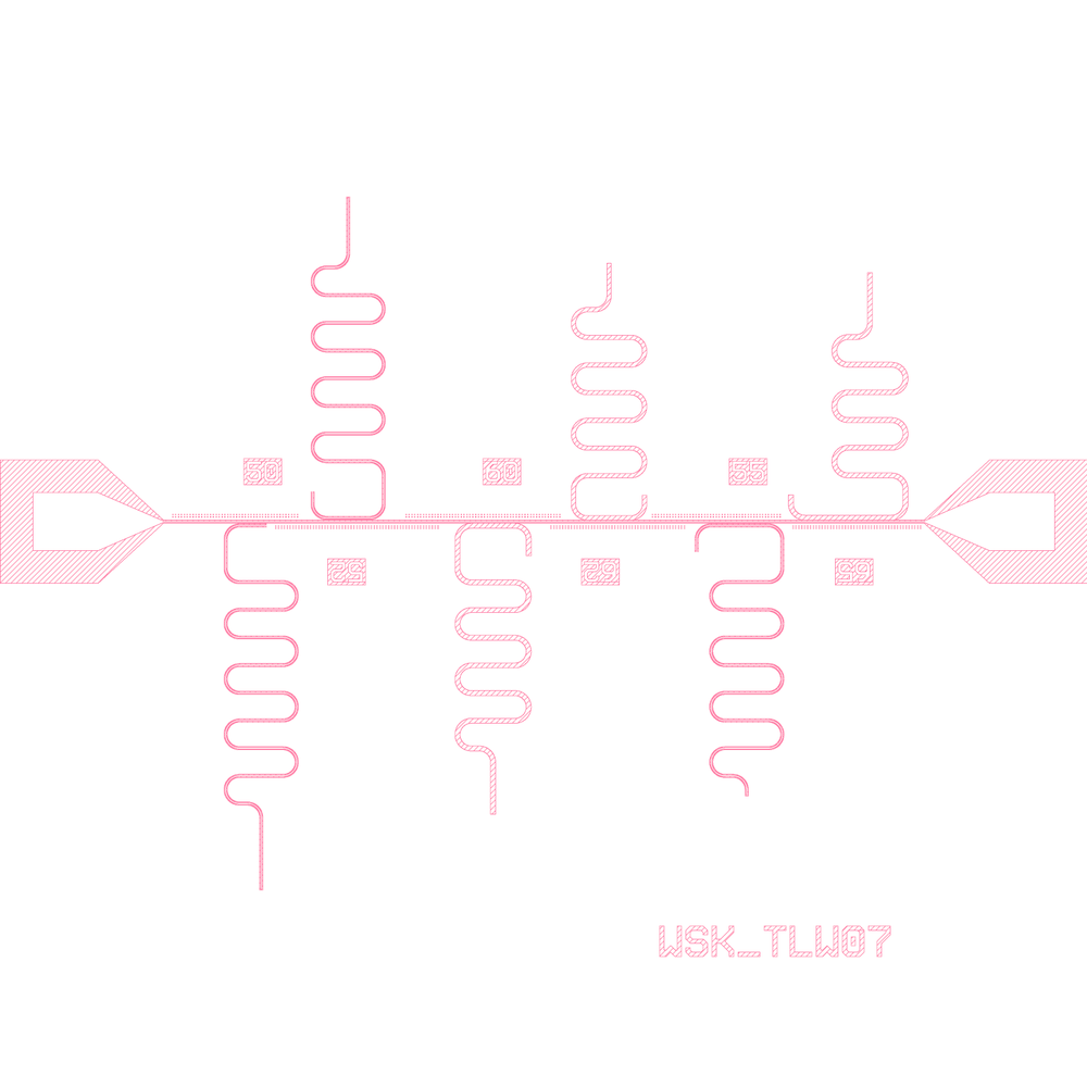
The original legacy layout (render of the legacy GDS), the older chip this one is checked against.
The rebuild on the Quantcore PDK: same resonators, now inside the die frame.
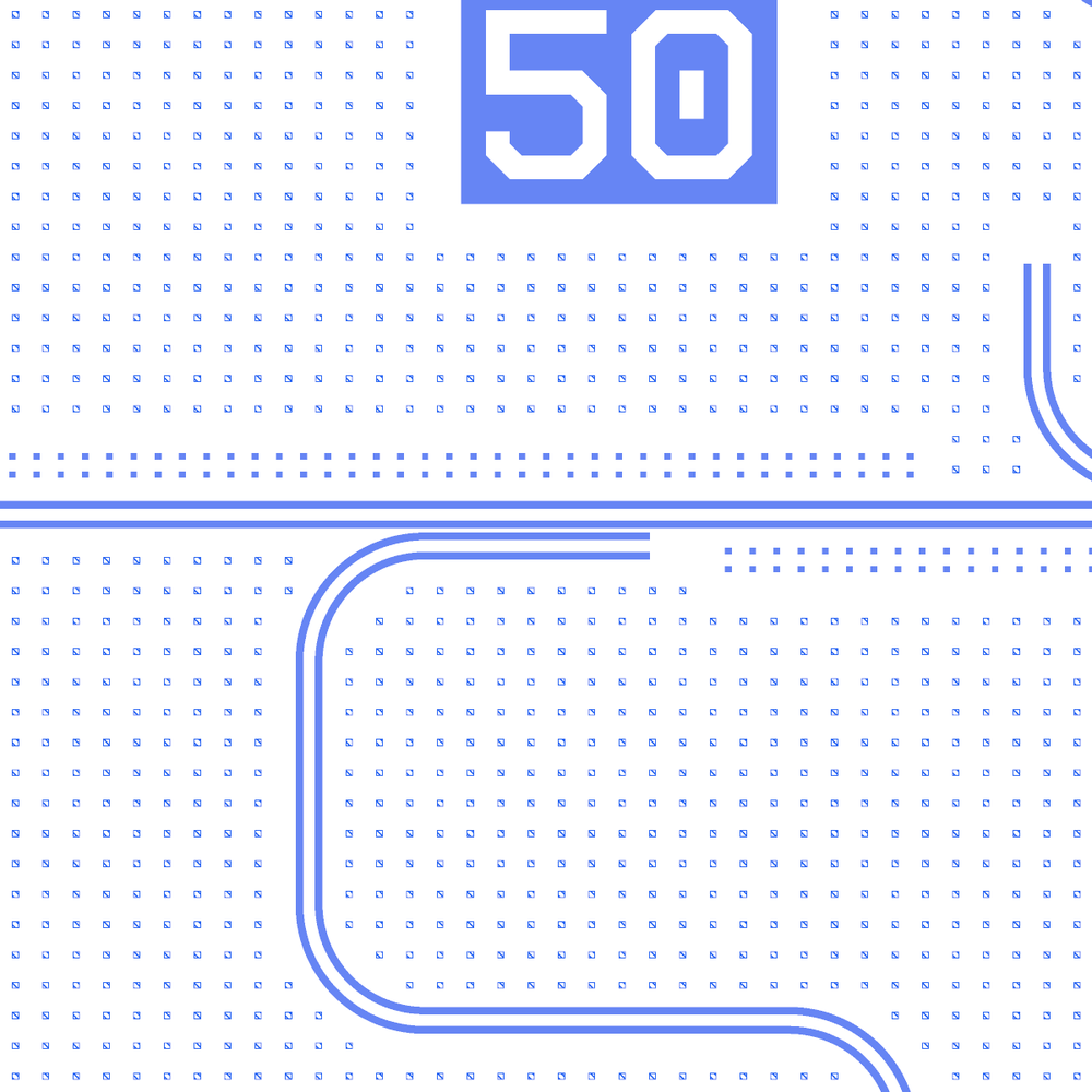
R2 (5.0 GHz): the straight coupling section sits 4 µm from the feedline; dotted rows are flux holes.

The left bond pad tapers into the 10 / 6 µm feedline.
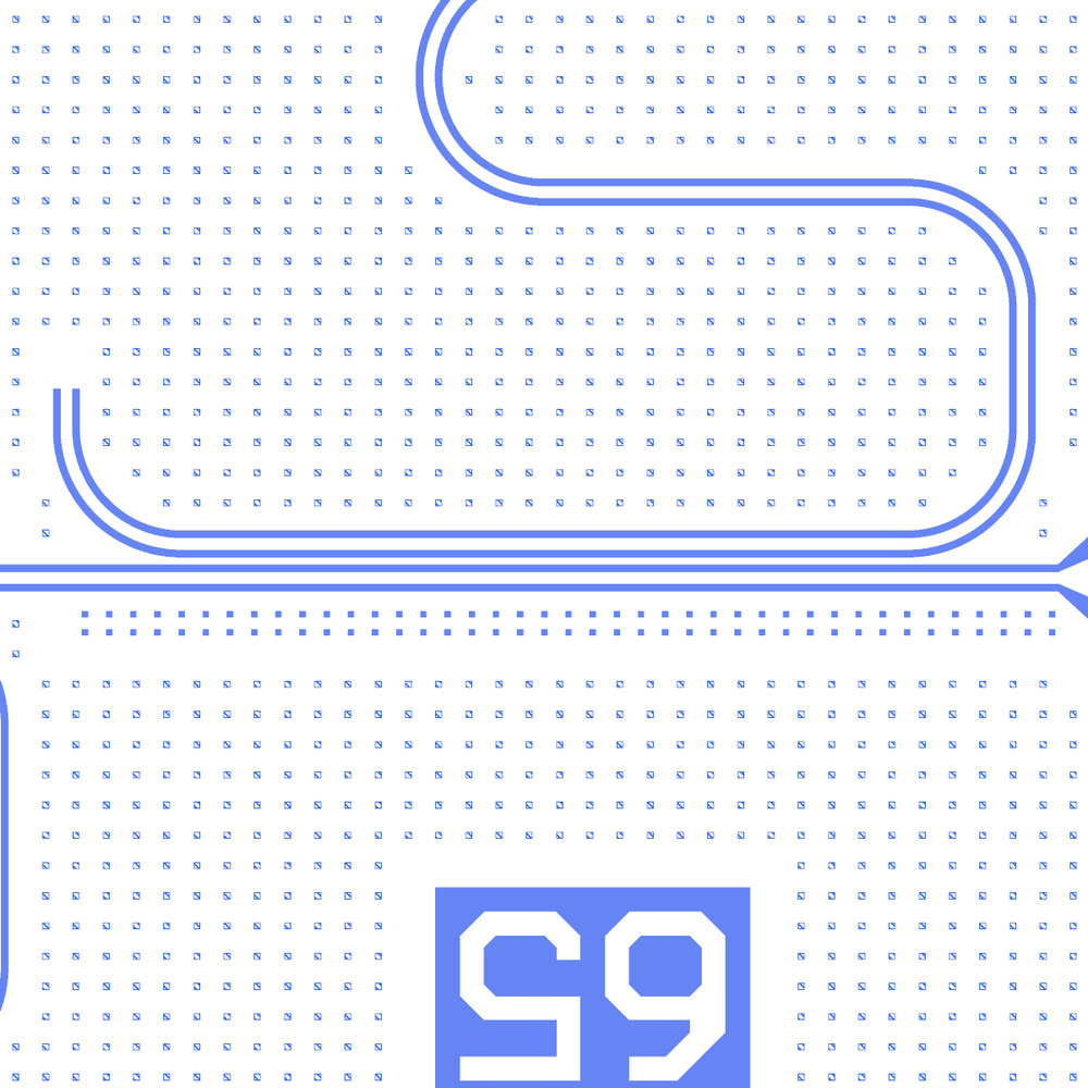
R12 (6.5 GHz) above the feedline, with its label 65 (mirrored) below.
LOM estimates
The notebook’s saved LOM table (one hanger resonator per row, no qubits). Target frequencies from the legacy labels are in brackets.
resonator |
f_r (GHz) (target) |
κ (MHz) |
|---|---|---|
R2 |
5.0682 (5.0) |
0.0538 |
R3 |
5.3719 (5.25) |
0.144 |
R6 |
5.6027 (5.5) |
0.289 |
R8 |
6.0352 (6.0) |
0.137 |
R9 |
6.3713 (6.25) |
0.24 |
R12 |
6.59 (6.5) |
0.701 |
These numbers are the notebook’s saved output, not re-run for this page. They are lumped-model estimates (component formulas and calibration), not FEM results; see the LOM page for how far to trust them.
Build spec
The rest of this page is the detailed spec the notebook was built from: every component, the changes made while rebuilding, and the notes.
Source: components/python/chip_07_resonators.py (create_test_chip, May 2024; output
chip_07_TLW4.0_6x_dec24), Quantcore internal. Legacy PCells: Coplanar Waveguide (CPW.lym), Connector Pad 2
(connector_pad_v2.lym), Coupled Resonator (CPW_Coupled_Resonator.lym), Marker (Marker.lym).
Rebuild: examples/designs/legacy/chip_07_resonators.ipynb (+ .json, PNGs); tables and the legacy reference
in examples/designs/legacy/_legacy_b.py (C07_*, chip07_reference).
Changes made in the rebuild
Targets: the legacy lengths and targets come from bare-resonator simulations without claws, and this chip’s resonators are bare; the 0.15–0.26 GHz offset of the written targets remains (lengths kept). No geometry change.
What it is: a resonator-only test chip (the header’s “10 resonators … and a couple of test junctions” is stale:
the code places six resonators; the test-pad block is commented out). A 5250 µm 10/6 µm feedline between two bond
pads carries six Coupled Resonators, three above and three below, each with a straight coupling section beside the
feedline (clength 200–600 µm, cgap 4–6 µm). Targets (code comments and the etched labels “50” … “65” = f × 10):
5.0, 5.25, 5.5, 6.0, 6.25, 6.5 GHz. Six flux-hole arrays line the feedline; text “WSK_TLW07” and six labels.
Die: 7.5 × 7.5 mm (hard-coded box_size), centred on (0, 0) → shifted by (+3750, +3750). The PDK v2 die frame
replaces the legacy Marker corners (thickness 50, width 500, rot 1/2/3/0 at the corners) and the 10/0 boundary
boxes (die outline and four 500 µm corner squares at (±3350, ±3350)). Legacy layers: 1/0 (etch), 3/0 (second-metal
envelope, fab_l), 10/0 (boundary).
Built; XOR with the legacy PCells is 0.0 µm² on every instance (see the second-metal note below).
Components
instance |
legacy cell |
catalog ref |
key params |
at (x, y) µm |
rot |
legacy (x, y), notes |
|---|---|---|---|---|---|---|
|
|
|
length 5250 (= 7500 − 2000 − 40 − 210), 10/6, lc/rc_thickness 2, c_gap 0 |
(3750, 3750) |
0 |
(0, 0) |
|
|
|
pad 400 × 450, pad_gap 225, taper (conn_height) 450, trace 10/6, round False |
(1125, 3750) |
270 (snapped to |
(−2625, 0) rot 3 |
|
|
|
as PL |
(6375, 3750) |
90 (snapped to |
(2625, 0) rot 1 |
|
|
|
cpw_len 6200, clength 200, cgap 4, neck 500, width 300, flip False |
(1750, 3724) |
0 |
(−2000, −26); 5.0 GHz |
|
|
|
cpw_len 5840, clength 300, cgap 4, neck 500, flip True |
(2400, 3776) |
0, mirror |
(−1350, 26); 5.25 GHz |
|
|
|
cpw_len 5590, clength 400, cgap 4, neck 500, flip True |
(5100, 3724) |
0 |
(1350, −26); 5.5 GHz |
|
|
|
cpw_len 5200, clength 300, cgap 6, neck 500 |
(3400, 3722) |
0 |
(−350, −28); 6.0 GHz; legacy second metal |
|
|
|
cpw_len 4920, clength 300, cgap 4, neck 400 |
(4200, 3776) |
0, mirror |
(450, 26); 6.25 GHz; legacy second metal |
|
|
|
cpw_len 4740, clength 600, cgap 6, neck 400, flip True |
(5850, 3778) |
0, mirror |
(2100, 28); 6.5 GHz; legacy second metal |
|
hole cell array ( |
|
5 µm holes, pitch 20 (x) × 15 (y), 2 rows, nx = 44 / 57 / 54 / 47 / 45 / 45 |
first hole at legacy (−2560, 33), (−1850, −45), (−950, 33), (50, −45), (750, 33), (1720, −45) |
0 |
holes on legacy 1/0 and 3/0 |
|
|
|
mag 300 |
(4550, 750) |
0 |
(800, −3000) |
|
|
|
inverted, mag 200 |
legacy x = −2050, −1250, −400, 500, 1300, 2250; y = +276 / −276 alternating |
0 / 180 |
the f × 10 labels |
– |
|
PDK die frame |
– |
– |
– |
replaced |
Common resonator parameters (resParams_common): cpw_len 4660 (overridden), gap 6, clength 300, cgap 4, width
300, flip False, neck_length 400, ground True (shorted at the coupler end in fab mode). The second, vertical
flux-hole table (rx/ry/ly lists after the first loop) is never inserted in the source: not drawn.
Second metal: R8, R9 and R12 are drawn with l = 3/0 and fab_l = 1/0, swapped from the
default, so in the legacy mask their CPW etch is on 3/0 and their 1/0 holds only the trace footprint grown by gap +
cgap (the base metal cleared under them: these three are patterned in the second metal; the header’s “4 on L3; 6
on L1”). PDK v2 derives 3/0 from 1/0 at export and has no per-element layer choice, so the rebuild draws all six
on 1/0. Against the true legacy 1/0 their XOR is the envelope (≈ 60 %); against the legacy PCells drawn with the
default layers it is 0.
Routes
None: the feedline is a CpwSegment, the pads snap to its ends, the resonators couple by proximity.
LOM node structure
FL.line: one node (feedline + both pads), 50 Ω port at each pad.Each
Ri: λ/4TLres(shorted at the coupler start, open atend; drawn length) fromRi.resto ground, and a HANGER κ element toFL.linedeclared with a value-lessd.couple("K_Ri", "Ri", "FL")(κ from clength / cgap).No qubits, no junctions. The
endports are the open ends (no route).
Targets
R2 5.0, R3 5.25, R6 5.5, R8 6.0, R9 6.25, R12 6.5 GHz (legacy comments; labels). The same lengths 4740, 4920, 5200, 5590, 5840 µm appear in design 14’s simulated calibration table (6.761, 6.525, 6.188, 5.787, 4.616 GHz).
Simplifications for a first rebuild
Second-metal resonators drawn on 1/0 (above).
PDK frame instead of the legacy markers and boundary boxes.