Two transmons and a bus (SQDMetal)
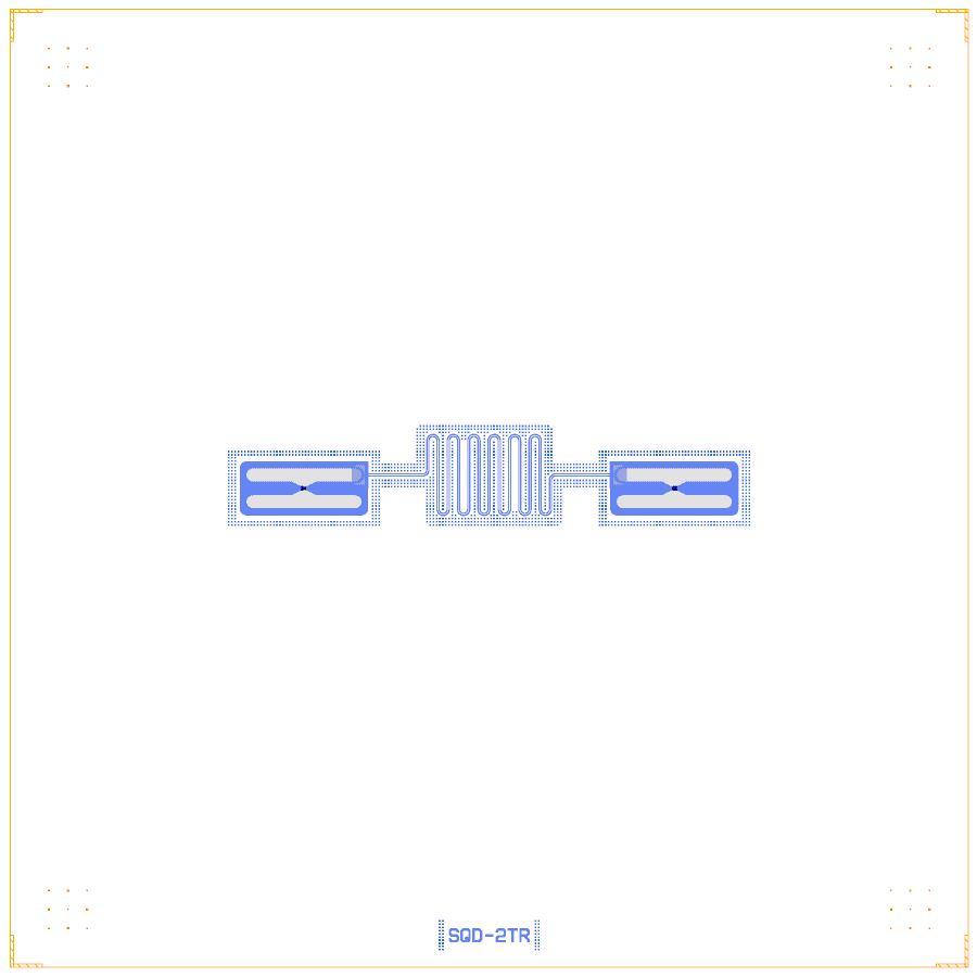
Two floating tapered-inset transmons, each coupled through a semicircular capacitor to a λ/2 bus resonator between them. There is no feedline. It is a bus-coupling study from the SQDMetal examples (Apache-2.0), rebuilt on the Quantcore PDK with the Quantcore re-implementations of TransmonTaperedInsets and the smooth capacitor.
Build this one to learn a qubit-bus-qubit chain without any pads, and how SQDMetal’s component options map to Quantcore cells.
At a glance
Notebook |
|
Source |
SQDMetal example |
Chip |
7.5 × 7.5 mm Quantcore die, the source’s 5 × 2 mm area in its middle |
On the chip |
2 tapered-inset transmons · 2 smooth semicircle capacitors · 1 λ/2 bus (6.8 GHz target) |
Builds today |
yes (layout built on 2026-11-19 in 9 s) |
How the notebook builds it
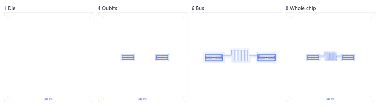
Die. The Quantcore die with the frame and the device ID.
Bond pads. None on this chip.
Readout line. None.
Qubits. Two
TransmonTaperedInsetswith the source’s options.Readouts. None.
Coupling. The two capacitors and the λ/2 bus between them.
Control lines. None.
Whole chip. Targets (f_q 4.5 GHz, bus 6.8 GHz), one sim group, centring, save.
LOM estimates
Numbers are from a run of this notebook on 2026-11-19 (Setup, Design, Check and the LOM cells, 10 s): QuCat normal modes with QuTiP dressed values.
parameter |
LOM (QuTiP) |
target |
|---|---|---|
|
4.51 |
4.5 |
|
-176 |
– |
|
-1.24 |
– |
|
4.52 |
4.5 |
|
-5.88 |
– |
|
6.56 |
6.8 |
|
0 |
– |
group |
pair |
ZZ (kHz) |
neighbours |
hybridised |
|---|---|---|---|---|
Q1-Q2 |
– |
yes |
yes |
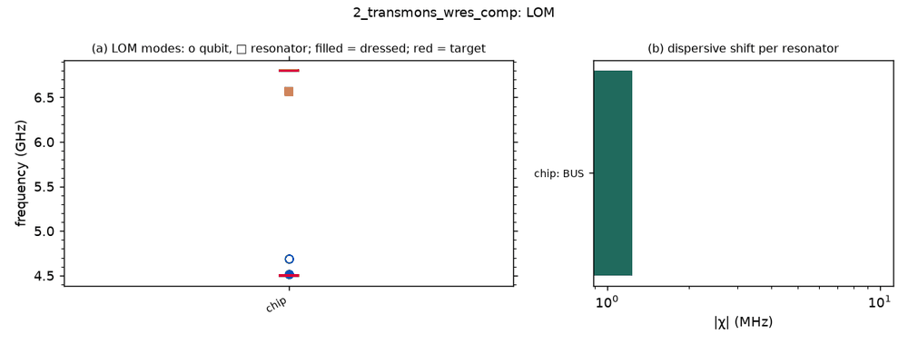
These are lumped-model estimates from component formulas and calibration, not FEM results. The LOM page says how far to trust them.
Build spec
The rest of this page is the detailed spec the notebook was built from: every component, port, route and length.
Source: doc-sphinx/source/examples/2_transmons_wRes_comp.ipynb
· SQDMetal components TransmonTaperedInsets (SQDMetal/Comps/Qubits.py), Smooth_Capacitor_Semicircle
(Comps/Test_capacitor.py), ResonatorMeanderPinPin · licence Apache-2.0 (verified) · read on 2026-11-02. Stored
outputs: layout plot, Palace capacitance matrix, derived circuit parameters.
What it is: two floating tapered-pad transmons on a 5 × 2 mm chip. Each is capacitively coupled, through a
semicircular “smooth” capacitor on its inner top pad corner, to a 8.96 mm λ/2 meander bus between them (6.8 GHz).
There is no feedline, and the chip is a bus-coupling study.
Frame: chip 5.0 × 2.0 mm centred at (0, 0), substrate 280 µm, silicon (siliconcryo). Box (0, 0, 5000, 2000),
Designer = source + (2500, 1000). CPW 10/6 µm.
TransmonTaperedInsets and Smooth_Capacitor_Semicircle have no KQC equivalent, so a first build uses stand-ins: DoublePads + its own coupler pad. The rebuild sections below use the Quantcore versions.
Components
instance |
catalog ref |
key params (units) |
at (x, y) Designer |
rot |
notes |
|---|---|---|---|---|---|
Qubit1 |
|
pads 800 × 110 (pad_width × pad_height), pad_gap 100 (island gap = junction length), pocket 1000 × 420 (pocket_height override; default 800), pocket_lower_tighten 0, taper 200 → 40 over 40 µm, inductor 20 × 36, charge-line pin offset (0, −10) |
(1250, 1000) |
0 (pads stacked in y) |
source (−1.25, 0) mm |
Qubit2 |
same |
same |
(4150, 1000) |
0 |
source (1.65, 0) mm |
Capacitor1 |
|
rect_width 160, rect_length 80, semi_radius 60, fillet 5 |
on Qubit1 |
180 |
|
Capacitor2 |
same |
same |
on Qubit2 |
0 |
Junctions: target L_J1 = 13.203 nH, L_J2 = 13.196 nH (E_J ≈ 12.38 GHz) for 4.5 GHz, so
junction={"Lj_nH": 13.2, "Cj_fF": 0}.
Routes
route |
from → to |
type, length |
notes |
|---|---|---|---|
Resonator1 |
Capacitor1.a → Capacitor2.a |
meander 8960 (λ/2 at 6.8 GHz on Si, 10/6 CPW, 200 nm film) |
|
Stand-in: d.route("BUS", Q1.cplr, Q2.cplr, meander=8960) with DoublePads rotated so cplr faces the bus (Q1
rot 270, Q2 rot 90). The coupler pad then plays the semicircle capacitor.
Launchers, pads, test structures, markers, labels
None.
LOM node structure
Q1, Q2: floating transmons, two islands each (C1/C2-ground ≈ 73.5 / 79.7 fF, Q-island pair C_Q ≈ 78.8 fF), JJ 13.2 nH. Each couples by C_g ≈ 7.1 fF to the bus resonator (λ/2, C_r ≈ 1446 fF to ground, modelled as L_res 745 pH ∥ C_res 735 fF at 6.8 GHz). Direct Q1–Q2 is negligible (E_Cc 0.18 MHz). No feedline or controls.
Targets (stated / computed)
f_q1 = f_q2 = 4.5 GHz · f_res 6.8 GHz · E_C ≈ 225.4 MHz · g1 ≈ 82.7 MHz, g2 ≈ 83.2 MHz (circuit-parameter block). The notebook’s second “coupled” block reports g ≈ 302 MHz with an uncoupled resonator at 30.3 GHz, which looks like a unit or setup slip. Use the first block.
Simplifications for a first rebuild
DoublePads (island extents [800, 110], island_island_gap 100, ground_gap [1000, 420], coupler_extent [160, 80]) as the stand-in. The tapered junction region and semicircle capacitor are cosmetic for a first LOM pass.
Wanted:
TransmonTaperedInsets(floating pads with tapered junction leads and corner pinstop_left_pin/top_right_pin/ …) andSmooth_Capacitor_Semicircle(rectangle + semicircle pad, pina).
Build with stand-ins
The stand-in build uses DoublePads (pads 800 × 110, gap 100, pocket 1000 × 420, 160 × 20 coupler plate 15 µm above the top pad), Q1 (1250, 1000), Q2 (4150, 1000) (source x −1.25 / +1.65 mm), bus 8960 µm leaving both pockets upward, meander (12 turns) between x 1850 and 3550.
Rebuild with TransmonTaperedInsets + SmoothCapacitorSemicircle
The DoublePads stand-ins are replaced by TransmonTaperedInsets (source options; pocket 1000 × 420) and
SmoothCapacitorSemicircle (160 × 80, r 60, fillet 5 / 20, orientation 180 / 0) snapped on top_right_pin /
top_left_pin. chrgln_pin_y_offset +10 (source −10 overlaps the qubit pad; 0 makes the DRC report open/short at
the pin on the pocket edge), lead_length 20. Bus = 8960 − 2 × (25 µm SQDMetal pin inset + 20 µm lead) = 8870 µm,
KQC meander, 12 turns. LOM (lom analytic: pads 126 fF to gnd, 37 fF pad–pad, capacitor 25 fF): f_q 4.06 / 4.06 GHz
hybridised (target 4.5), bus 6.67 GHz (target 6.8 on Si), χ −0.96 MHz (with the stand-ins: 4.59 GHz / 6.86 GHz).
Open issue: the Q3D export merges each qubit’s two pads (junction port has no edge).
Quantcore PDK rebuild
The notebook is a Quantcore PDK rebuild of the source, not a replica: the netlist, LOM and imported components are kept, and the process is Quantcore’s.
Notebook: examples/designs/sqdmetal/2_transmons_wres_comp.ipynb.
Chip: the Quantcore die frame (L dicing markers 1000/0, 3 × 3 alignment grids 1001/0, chip boundary 100/0, device ID where an edge is free; any brand text is QCT), on the 7.5 × 7.5 mm Quantcore die; the source’s 5 × 2 mm chip area is centred in it (
box=(-1250, -2750, 6250, 4750)), so every coordinate stays the source’s.Stack: sapphire 650 µm, εr 10.25 (the PDK default stack, used by the LOM estimates and every FEM export); the SQDMetal examples are on silicon (280–500 µm), so frequencies differ from the source’s.
Junctions: Quantcore Nb/AlOx/Nb trilayer junctions (
junction_typefromlayouts.registry.trilayer_junction): fingers on 2/0 + 4/0, spacer 50/0 with the 51–53/0 gradient, sized on the PDK junction rule (Nb Δ = 1.4 meV, I_c·R_n = πΔ/2e, R_n·A 13.5 kΩ·µm² and C_J 50 fF/µm² assumed). Both junctions are sized for the stated f_q 4.5 GHz with each qubit’s LOM C_Σ (≈ 107 fF): straight fingers 0.34 µm × 0.6 µm, L_J ≈ 9.9 nH, C_J ≈ 10.2 fF, so R_n ≈ 67 kΩ, above the 40–50 kΩ window (a 45 kΩ junction would put them at ≈ 5.4 GHz). Drawn across the 20 µm taper-tip gap byTransmonTaperedInsets(junction_params); cell 1 prints the sizing.Kept: the topology (two floating transmons, a λ/2 bus through two smooth capacitors), the components with the source’s options and positions, the bus length, the targets, the sim group.