10 × 10 package array (tutorial 4.43)
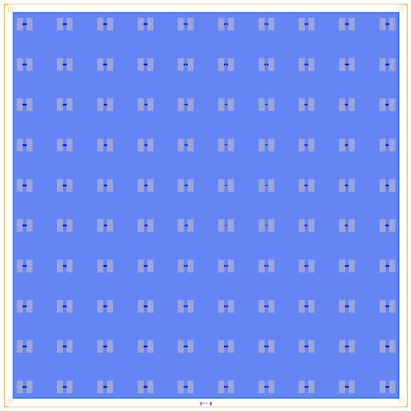
One hundred bare two-paddle transmons on a 3 mm pitch, on a 30 × 30 mm chip with no ground plane. There are no routes, resonators or ports. The chip is the validation processor of a package-mode study (Molavi et al.), meant to be meshed and solved with its metal box. It is the layout of Qiskit Metal tutorial 4.43 (Apache-2.0, © Qiskit Metal contributors). The Quantcore rebuild is distributed under GPL-3.0.
Build this one to see a chip made of bare paddles only, and how the PDK frame sits on a chip whose ground is a separate etch. The qubits are uncoupled in the circuit and couple only through the package modes.
At a glance
Notebook |
|
Source |
Qiskit Metal |
Chip |
30 × 30 mm (the source’s size, far larger than the 7.5 mm Quantcore die) |
On the chip |
100 two-paddle transmons (two 0.5 × 1 mm paddles, 0.2 mm gap) · a chip-wide ground etch 0.7 mm inside the die edge |
Builds today |
yes (layout built on 2026-11-19 in 6 s) |
How the notebook builds it
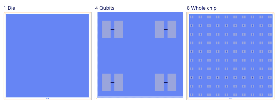
Die. A 30 mm square with the QCT frame and the chip-wide ground etch.
Bond pads. None.
Readout line. None.
Qubits. One hundred two-paddle transmons (the picture zooms on four of them).
Readout resonators. None.
Coupling. None: there are no routes; the qubits couple only through the package modes.
Control lines. None.
Whole chip. Sim groups for the FEM jobs (one qubit, and a 2 × 2 corner), the content centred in the die, the design saved.
LOM estimates
Numbers are from the .v1 notebook’s saved output (the 10 × 10 array was not re-run for these docs). The 100 transmons are identical and uncoupled in the LOM, so only Q_0_0 is solved.
group |
qubit |
f_q (GHz) |
α (MHz) |
resonator |
f_r (GHz) |
κ (MHz) |
χ (MHz) |
|---|---|---|---|---|---|---|---|
Q_0_0 |
Q_0_0 |
4.046 |
-72.1 |
– |
– |
– |
– |
The LOM puts about 408 fF per pad to ground because its TwoPadTransmon model assumes a ground plane, which this package chip does not have: the LOM’s C across the junction is 261 fF against the paper’s fit of 173.8 fF, so f_q is underestimated and the paper’s value is the reference.
These are lumped-model estimates from component formulas and calibration, not FEM results. The LOM page says how far to trust them.
Build spec
The rest of this page is the detailed spec the notebook was built from: every component, port, route and length.
The notebook
examples/designs/metal/tut443_10x10_package.ipynbuses the qccTwoPadTransmon(500 × 1000 pads, 200 gap, no leads, no pocket) on a chip-widemetal:Rectangle subtract(no ground plane).
Source: Quantum Metal docs/tut/4-Analysis/4.43-Mesh-and-solve-the-10x10-processor.ipynb. The layout is built by
docs/tut/resources/package_modes/package_modes.py (build_design, TwoPadTransmon, DEVICE, PAPER) and shared
by tutorials 4.41–4.46. Licence Apache-2.0. Paper: R. Molavi et al., “Extracting electromagnetic bare mode
couplings in large superconducting quantum processors”, arXiv:2609.22442 (2026), validation device of Fig. 4.
This is a package-mode study and has no wiring. It has 100 bare two-paddle transmons on 0.5 mm silicon in a
30 × 30 × 3 mm metal box, with no ground plane, no resonators and no ports. Each junction is a line across the
paddle gap (a lumped L in the solver).
Chip 30 000 × 30 000 µm, already spanning 0…30 mm (Metal center = (15, 15) mm), so Designer = Metal + (0, 0).
It is a MultiPlanar design: metal thickness 0, substrate 0.5 mm, lid at 3 mm (sample_holder_top 2.5 mm above the
chip).
The build needs a ground-plane-free two-paddle transmon (the qcc TwoPadTransmon) and a chip without ground metal.
Components (generator)
for i in range(10):          # column, x
    for j in range(10):      # row, y
        d.add(f"Q_{i}_{j}", "MISSING:TwoPadTransmon", at=((i + 0.5) * 3000, (j + 0.5) * 3000), rot=0,
              pad_width=500, pad_height=1000, pad_gap=200)   # junction line across the gap, jj_width 20
param |
value |
meaning |
|---|---|---|
pitch |
3000 µm in x and y |
qubit (i, j) centre at ((i + 0.5)·3, (j + 0.5)·3) mm |
paddle |
500 (x, junction direction) × 1000 (y) µm |
two paddles side by side along x |
gap |
200 µm |
the junction length; JJ drawn as a line from (−100, 0) to (+100, 0) |
orientation |
0 |
|
substrate |
Si, εr 11.9, 0.5 mm |
|
box |
30 × 30 × 3 mm |
package walls are the boundary |
Routes
None.
Launchers, pads, test structures, markers, labels
None. There is no ground plane, so the paddles float in the box.
LOM node structure
Each of the 100 qubits is a two-island transmon (C_n, C_m and junction L). All of them couple to the package modes (LSM110 at about 6.48 GHz with paddles, LSM210 at about 10.23 GHz). Qubit–qubit couplings come only through the box modes and the direct cross-capacitance. This is not a Designer LOM circuit (feedline/resonator), so model it with the package-mode solver.
Targets (if stated)
quantity |
value (paper) |
|---|---|
empty box / with Si / with paddles |
7.07 / 6.49 / 6.48 GHz |
qubit C |
≈ 170 fF |
shunt L (impedance-matrix method) |
3.6 nH |
dipole moment (1 J) |
3.41e-10 C·m, dipole length 0.58 mm |
coupling amplitude A_110 / A_210 |
15.6 / 49.8 MHz (fit) |
2g of qubit (1, 1) |
12.6 MHz |
Mesh seeds: h_metal 0.1 mm, h_max 1 mm, optional h_junction 0.05 mm.
Simplifications for a first rebuild
For a Designer stand-in, use KQC
DoublePads(island1_extent=[1000, 500], island2_extent=[1000, 500], island_island_gap=200)rotated so the islands sit side by side along x, with a largeground_gap(~2800 µm). This is still grounded, so the package-mode physics differs.A faithful version needs a
TwoPadTransmoncell (two rectangles plus a junction line, no ground cut-out) and a chip option with the ground plane removed (cf. KQCEmptychip).
Quantcore PDK rebuild
The notebook is a Quantcore PDK rebuild of the source, not a replica: the netlist, LOM and imported components are kept, and the process is Quantcore’s.
Notebook: examples/designs/metal/tut443_10x10_package.ipynb.
Chip: the Quantcore die frame (L dicing markers 1000/0, 3 × 3 alignment grids 1001/0, chip boundary 100/0, device ID where an edge is free; any brand text is QCT), drawn on the source’s 30 × 30 mm chip. The source has no ground plane; the rebuild keeps the chip-wide etch but stops it 0.7 mm inside the die edge, so the frame’s dicing L’s and alignment grids sit in ground metal (the paddles start 1.25 mm from the edge). That rim is the only ground plane, so the PDK cheese band (chip
cheese: "auto") is a dotted line of holes along the inside of the rim; the 100 transmon pads are isolated metal and stay solid.Stack: sapphire 650 µm, εr 10.25 (the PDK default stack, used by the LOM estimates and every FEM export); the source uses 0.5 mm silicon in a 3 mm metal box, so the LOM capacitances, resonator frequencies and FEM jobs here are for sapphire rather than the source’s substrate.
Junctions: every
TwoPadTransmoncarries a Quantcore trilayer junction across the 200 µm gap (junction_type="Quantcore Junction",junction_params={"lj_nH": 5.3448}; drawn window 200 × 32 µm). Sizing: 4.05 GHz target (C_Σ ≈ 261 fF across the gap), L_J ≈ 5.4 nH, C_J ≈ 19 fF, so R_n ≈ 36 kΩ, just below the 40–50 kΩ window (the paper’s fit was 3.63 nH).Kept: the topology (100 bare two-paddle transmons on a 3 mm pitch), positions, paddle sizes, gap, orientation, the sim groups.