Barends five-qubit (Metal 52)
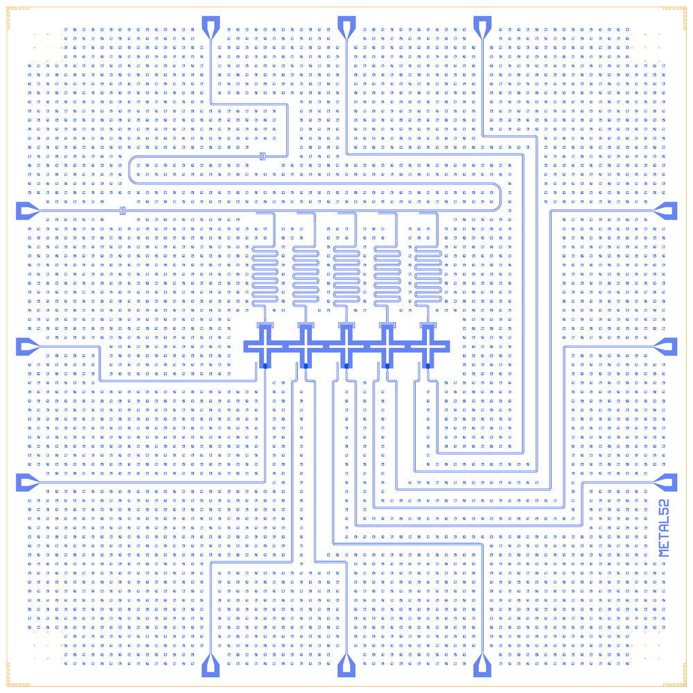
Five Xmon qubits sit in a line, close enough that neighbours couple directly through their facing cross arms. Each has its own λ/4 readout meander on a shared feedline (whose middle section acts as a Purcell filter), an XY drive line and a Z flux line. It is the Qiskit Metal “52” example (Apache-2.0, © IBM and contributors), a layout inspired by Barends et al. (Nature 508, 500, 2014), not the fabricated mask. The Quantcore rebuild is distributed under GPL-3.0.
Build this one to learn direct qubit-qubit coupling without bus resonators, multiplexed readout with staggered resonator lengths, and a full set of drive and flux lines on a 7.5 mm die.
At a glance
Notebook |
|
Source |
Qiskit Metal |
Chip |
7.5 × 7.5 mm Quantcore die (the source’s 6 × 6 mm area centred in it), CPW 10 / 6 µm |
On the chip |
5 flux-tunable Xmons (450 µm pitch) · 5 λ/4 readouts (4.41 to 4.57 mm) · 5 coupled-line tees · 2 Purcell capacitors · 5 XY and 5 Z lines · 12 bond pads |
Builds today |
yes (layout built on 2026-11-19 in 13 s) |
How the notebook builds it
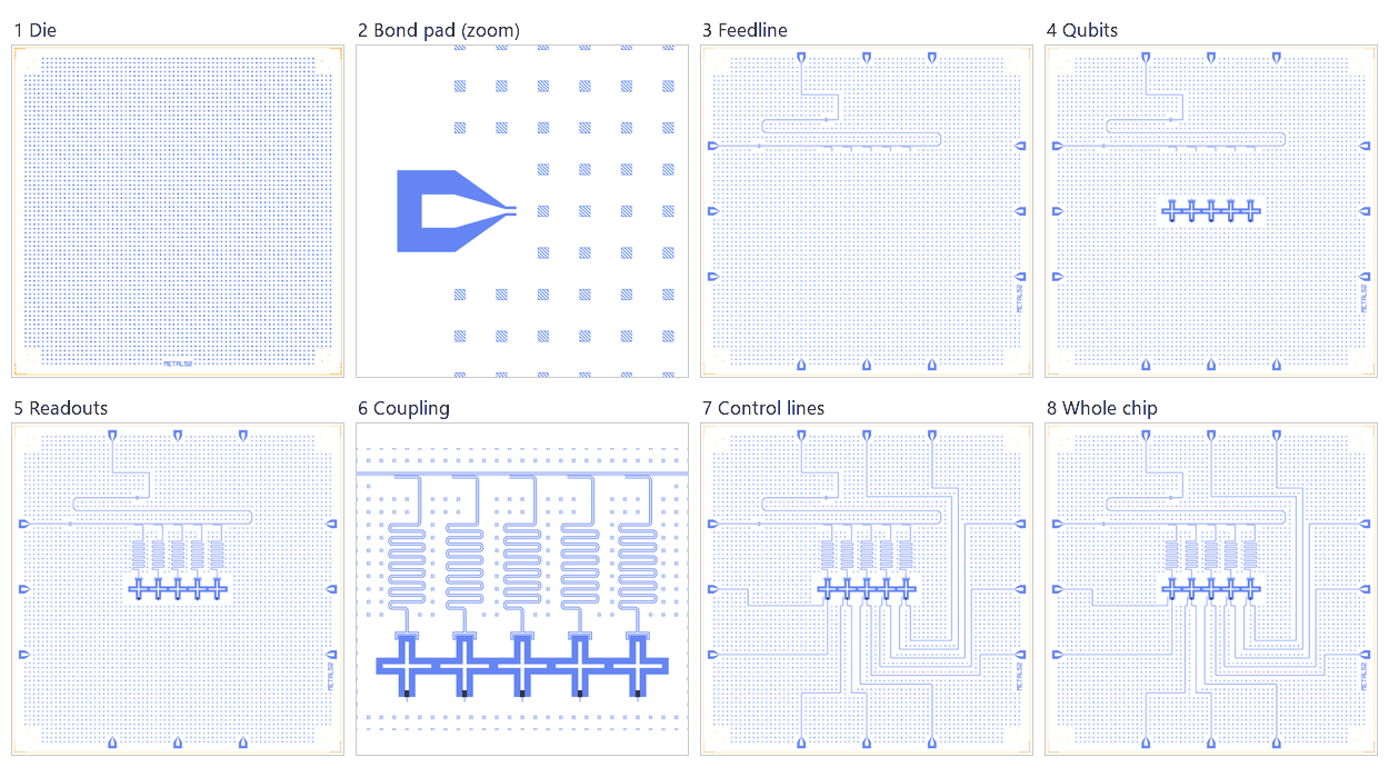
Die. The 7.5 mm die with the QCT frame (dicing marks, alignment grids, chip boundary, device ID).
Bond pads. Twelve launchpads, three per edge, slid to the 100 µm pad-edge rule (the picture zooms on one pad).
Feedline. Five coupled-line tees, two Purcell series capacitors and the feedline between the input and output pads.
Qubits. Five Metal crossmons with Quantcore SQUIDs, 450 µm apart.
Readout resonators. Five λ/4 meanders from each qubit’s claw to its tee.
Coupling. The four direct neighbour couplings, declared in the netlist (the picture zooms on the qubits).
Control lines. An XY line ending open beside each cross and a Z flux line for each qubit, to the edge pads.
Whole chip. Sim groups for the FEM jobs (the qubit chain and the readout), the content centred in the die, the design saved.
LOM estimates
Numbers are from a run of this notebook on 2026-11-19 (Setup, Design, Check and the LOM cells, 38 s): QuCat normal modes with QuTiP dressed values.
group |
qubit |
f_q (GHz) |
α (MHz) |
resonator |
f_r (GHz) |
κ (MHz) |
χ (MHz) |
|---|---|---|---|---|---|---|---|
Q0+R0 |
Q0 |
6.357 |
-277 |
CLT0 |
6.275 |
0 |
28 |
Q1+R1 |
Q1 |
6.352 |
-272 |
CLT1 |
6.23 |
0 |
23.3 |
Q2+R2 |
Q2 |
6.35 |
-266 |
CLT2 |
6.183 |
0 |
23.9 |
Q3+R3 |
Q3 |
6.348 |
-273 |
CLT3 |
6.136 |
0 |
30.2 |
Q4+R4 |
Q4 |
6.348 |
-212 |
CLT4 |
6.089 |
0 |
-31.3 |
group |
pair |
ZZ (kHz) |
neighbours |
hybridised |
|---|---|---|---|---|
chain |
Q1-Q2 |
– |
yes |
yes |
chain |
Q0-Q2 |
– |
no |
yes |
chain |
Q2-Q4 |
– |
no |
yes |
chain |
Q2-Q3 |
– |
yes |
yes |
chain |
Q0-Q1 |
– |
yes |
yes |
chain |
Q1-Q4 |
– |
no |
yes |
chain |
Q1-Q3 |
– |
no |
yes |
chain |
Q0-Q4 |
– |
no |
yes |
chain |
Q0-Q3 |
– |
no |
yes |
chain |
Q3-Q4 |
– |
yes |
yes |
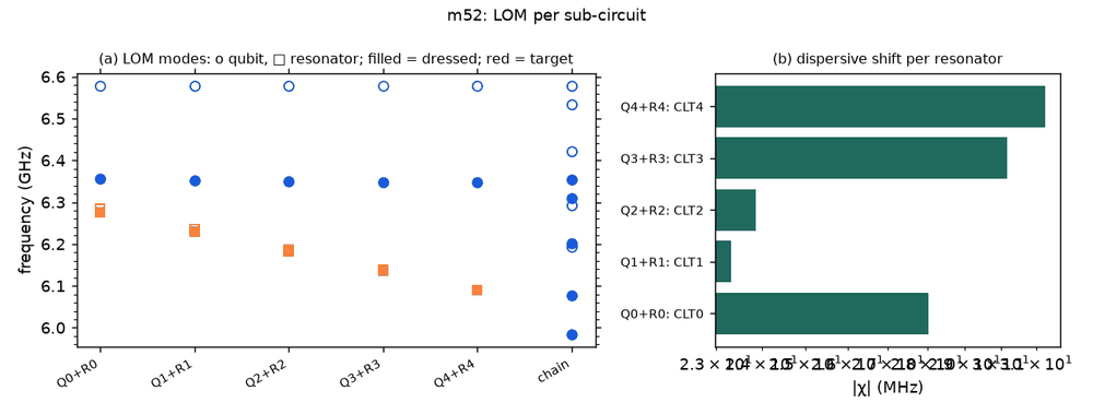
These are lumped-model estimates from component formulas and calibration, not FEM results. The LOM page says how far to trust them.
Build spec
The rest of this page is the detailed spec the notebook was built from: every component, port, route and length.
The
metal:references in this spec build as written, through themetal:wrapper (ports are the Metal pin names, parameters the Metal options). The Quantcore and KQC substitutions are optional.
Source: Quantum Metal docs/circuit-examples/F.Small-quantum-chips/52-Barends_5Qubit_Xmon_Processor.ipynb.
Licence Apache-2.0. The notebook adapts the QDW 2026 capstone solution by M. C. Sarihan, after Barends et al.,
Nature 508, 500 (2014). The notebook calls it “a physical-layout example inspired by the published device, not the
fabricated mask”.
The chip has five TransmonCrossFL Xmons in a 1-D chain at 450 µm pitch. Their ground pockets overlap, so neighbours
couple directly through the arm capacitance and there are no bus resonators. Each qubit has a λ/4 meander readout
shorted at a CoupledLineTee on one feedline. The feedline section between two CapNInterdigital series caps acts
as a common Purcell filter. Each qubit also has an XY drive line (open end) and a Z flux line, each going to its own
edge pad.
Chip 6000 × 6000 µm, centred, so Designer = Metal + (3000, 3000). CPW 10/6 µm except the Z-line pin (5 µm); all
routes in the source use 10/6. Metal layer 1. The junctions are left out of the GDS (no junction file).
A first build uses these substitutions: Xmon with flux_port, hanger for CoupledLineTee, KQC
FingerCapacitorSquare for CapNInterdigital, BondPad, and free ends for the XY lines.
Components
instance |
catalog ref |
key params (µm) |
at (x, y) |
rot |
notes |
|---|---|---|---|---|---|
Q0 … Q4 |
|
Metal cross_width 30, cross_length 190 (arm), cross_gap 50 → Xmon |
(2100 + 450 i, 3000) |
0 |
readout claw north (Metal connector_location 90); flux T-line south (t_top 15, t_width 5, t_gap 3, t_inductive_gap 3) |
CLT0 … CLT4 |
hanger on FL_P (metal:CoupledLineTee) |
coupling_length 200, coupling_space 4, down_length 100, open_termination False (short) |
centre (2100 + 450 i, 4500) |
0 |
second line below the feed; leg at x + 100 |
XY0 … XY4 |
free end (metal:OpenToGround) |
width 10, gap 6, termination_gap 6 |
(2000 + 450 i, 2820) |
— |
open drive end SW of each cross |
CAP_IN |
KQC |
Metal: 5 fingers × 20 µm, cap_width 10, cap_gap 6, cap_distance 50 |
(527, 4500) |
0 |
Metal span 454–600; a faces W, b faces E |
CAP_OUT |
KQC |
same |
(2073, 5100) |
0 |
Metal span 2000–2146 |
LP_W1, W2, W3 |
|
Metal default pad |
(225, 1500), (225, 3000), (225, 4500) |
270 |
|
LP_E1, E2, E3 |
|
same |
(5775, 1500), (5775, 3000), (5775, 4500) |
90 |
|
LP_S1, S2, S3 |
|
same |
(1500, 225), (3000, 225), (4500, 225) |
0 |
|
LP_N1, N2, N3 |
|
same |
(1500, 5775), (3000, 5775), (4500, 5775) |
180 |
Routes
route |
from → to |
type, length |
waypoints / hanger |
notes |
|---|---|---|---|---|
FL_IN |
LP_W3.a → CAP_IN.a |
cpw ≈ 265 |
— |
Metal Feed_in_lp |
FL_P |
CAP_IN.b → CAP_OUT.a |
cpw ≈ 10 030 |
nodes [(4700, 4500), (4700, 4800), (600, 4800), (600, 5100)] |
Purcell section; straight y = 4500 run carries the five hangers |
FL_OUT |
CAP_OUT.b → LP_N1.a |
cpw ≈ 1695, r = 20 |
nodes [(2346, 5100), (2346, 5675), (1500, 5675)] |
Metal lead 200/100 |
R0 … R4 |
Qi.claw_n → |
meander 4710 + 40 i |
— |
Metal total_length 4.41–4.57 mm + 300 µm CLT (down leg + coupler); spacing 50, fillet 20 |
XY0 |
LP_W2.a → |
cpw 2329, r = 20 |
[(275, 3000), (275, 2620), (2000, 2620)] |
the XY rows below are Metal RouteFramed paths, reversed |
Z0 |
LP_W1.a → Q0.flux |
cpw 3088 |
[(2100, 1500)] |
|
XY1 |
LP_S1.a → |
cpw 3511 |
[(1500, 620), (2400, 620), (2400, 2620), (2450, 2620)] |
|
Z1 |
LP_S2.a → Q1.flux |
cpw 2912 |
[(3000, 622), (2650, 622), (2650, 2622), (2550, 2622)] |
|
XY2 |
LP_S3.a → |
cpw 4261 |
[(4500, 820), (2850, 820), (2850, 2620), (2900, 2620)] |
|
Z2 |
LP_E1.a → Q2.flux |
cpw 4911 |
[(5600, 1500), (5600, 1021), (3100, 1021), (3100, 2622), (3000, 2622)] |
|
XY3 |
LP_E2.a → |
cpw 5862 |
[(5400, 3000), (5400, 1220), (3300, 1220), (3300, 2620), (3350, 2620)] |
|
Z3 |
LP_E3.a → Q3.flux |
cpw 6661 |
[(5250, 4500), (5250, 1422), (3550, 1422), (3550, 2622), (3450, 2622)] |
|
XY4 |
LP_N3.a → |
cpw 7303 |
[(4500, 5320), (5100, 5320), (5100, 1620), (3750, 1620), (3750, 2620), (3800, 2620)] |
|
Z4 |
LP_N2.a → Q4.flux |
cpw 7802 |
[(3000, 5122), (4950, 5122), (4950, 1822), (4000, 1822), (4000, 2622), (3900, 2622)] |
Hanger geometry: the feed travels +x, the resonators hang below (right), and the tee’s leg is at the downstream end
with the short upstream, which is why direction="backward". s is measured from CAP_IN.b at x = 563.5.
ground_gap 4 = |Δy| 26 − 5 − 6 − 5 − 6. The control lines in the source are laid out without crossings. Use
r=20 (Metal fillet 20) on the short jogs.
Launchers, pads, test structures, markers, labels
There are 12 pads, 3 per edge on a 1.5 mm pitch. The feed enters at LP_W3 and leaves at LP_N1. XY: W2, S1, S3, E2, N3. Z: W1, S2, E1, E3, N2. There are no markers or labels.
LOM node structure
Q0–Q4: Xmon islands, each with a JJ to ground. Nearest neighbours share a direct island–island C. That coupling is geometric, so it needs a FEM C-matrix; the component estimates miss it.
R0–R4: λ/4 resonators, open at the claw (C_g) and shorted at the hanger, with a coupled-line κ to FL_P.
FL_P: a λ/2 Purcell filter (~10.0 mm) between CAP_IN and CAP_OUT (series C), which go to the 50 Ω ports LP_W3 / LP_N1.
Control: XYi is an open drive line with C_d to island i (port LP_). Zi* is a flux line to the junction (
fluxport). Use a SQUID (TrilayerSquid) if flux tuning is modelled.
Targets (if stated)
The only stated design choice is the staggered readout lengths, 4.41–4.57 mm in 0.04 mm steps, for distinct
multiplexed tones. No Lj/Cj is set, so take the Metal default Lj 10 nH: junction={"Lj_nH": 10, "Cj_fF": 2}.
Simplifications for a first rebuild
Build the feed as three routes (FL_IN, FL_P, FL_OUT) with the Purcell loop nodes. Hang all five resonators on FL_P.
Use FingerCapacitorSquare for both CapNInterdigital caps. They are shorter (73 µm) than Metal’s 146 µm, so centre them at the Metal midpoints given above.
Make each XY line a free end with
term=6. Route each Z line toXmon.flux(port end, so the tip shorts to ground).The ground pockets overlap at 450 µm pitch. If the DRC flags the merged gaps, keep the pitch (it carries the direct coupling) and waive the warning, or raise the pitch to 480 µm.
Quantcore PDK rebuild
The notebook is a Quantcore PDK rebuild of the source, not a replica: the netlist, LOM and imported components are kept, and the process is Quantcore’s.
Notebook: examples/designs/metal/m52_barends_5q.ipynb.
Chip: the Quantcore die frame (L dicing markers 1000/0, 3 × 3 alignment grids 1001/0, chip boundary 100/0, device ID where an edge is free; any brand text is QCT), on the 7.5 × 7.5 mm Quantcore die; the source’s 6 × 6 mm chip area is centred in it (
box=(-750, -750, 6750, 6750)), so every coordinate stays the source’s (the source’s 6 × 6 mm, drawn 6.2 × 6.2 mm with the overhanging pads, fits).Stack: sapphire 650 µm, εr 10.25 (the PDK default stack, used by the LOM estimates and every FEM export); Metal’s
DesignPlanardefault is silicon (εr 11.45, 750 µm), so the LOM capacitances, resonator frequencies and FEM jobs here are for sapphire rather than the source’s substrate.Junctions: Quantcore Nb/AlOx/Nb trilayer junctions (
junction_typefromlayouts.registry.trilayer_junction): fingers on 2/0 + 4/0, spacer 50/0 with the 51–53/0 gradient, sized on the PDK junction rule (Nb Δ = 1.4 meV, I_c·R_n = πΔ/2e, R_n·A 13.5 kΩ·µm² and C_J 50 fF/µm² assumed); the fiveTransmonCrossFL(XY + Z lines) each get a PDK SQUID of two 0.25 × 0.6 µm junctions → R_n = 45 kΩ in parallel, L_J = 6.73 nH at zero flux, C_J = 15 fF (in the 40–50 kΩ window) (the source has nohfss_inductanceand leaves the junctions out of its GDS). Expected f_q ≈ 6.3 GHz (an estimate), close to the 6.2–6.4 GHz readouts, so the rebuild’s frequency plan needs the Z lines (or a resized junction) to detune them. The five qubits stay identical.Kept: the topology and every Metal component with the source’s options (through the
metal:wrapper), positions and orientations, every route’s end pins and total length, the sim groups (the feedline with its Purcell section, the five λ/4 readouts 4410–4570 µm, the ten XY / Z lines, thed.couplearm-to-arm estimate).