DeviceLayout SingleTransmon
A single grounded rectangular transmon island read out through a λ/4 meander that ends in a claw. The meander is coupled to a straight feedline over 400 µm and is shorted at the far end. It is the DeviceLayout.jl SingleTransmon example (AWS, MIT), built there as a Palace eigenmode model, and is rebuilt here on the Quantcore PDK (the rebuild is distributed under GPL-3.0).
This is the smallest complete readout: a feedline between two pads, one qubit with a claw, and one hanger resonator. The junction is re-sized for 4.05 GHz because the source’s 3.37 GHz is below the PDK band.
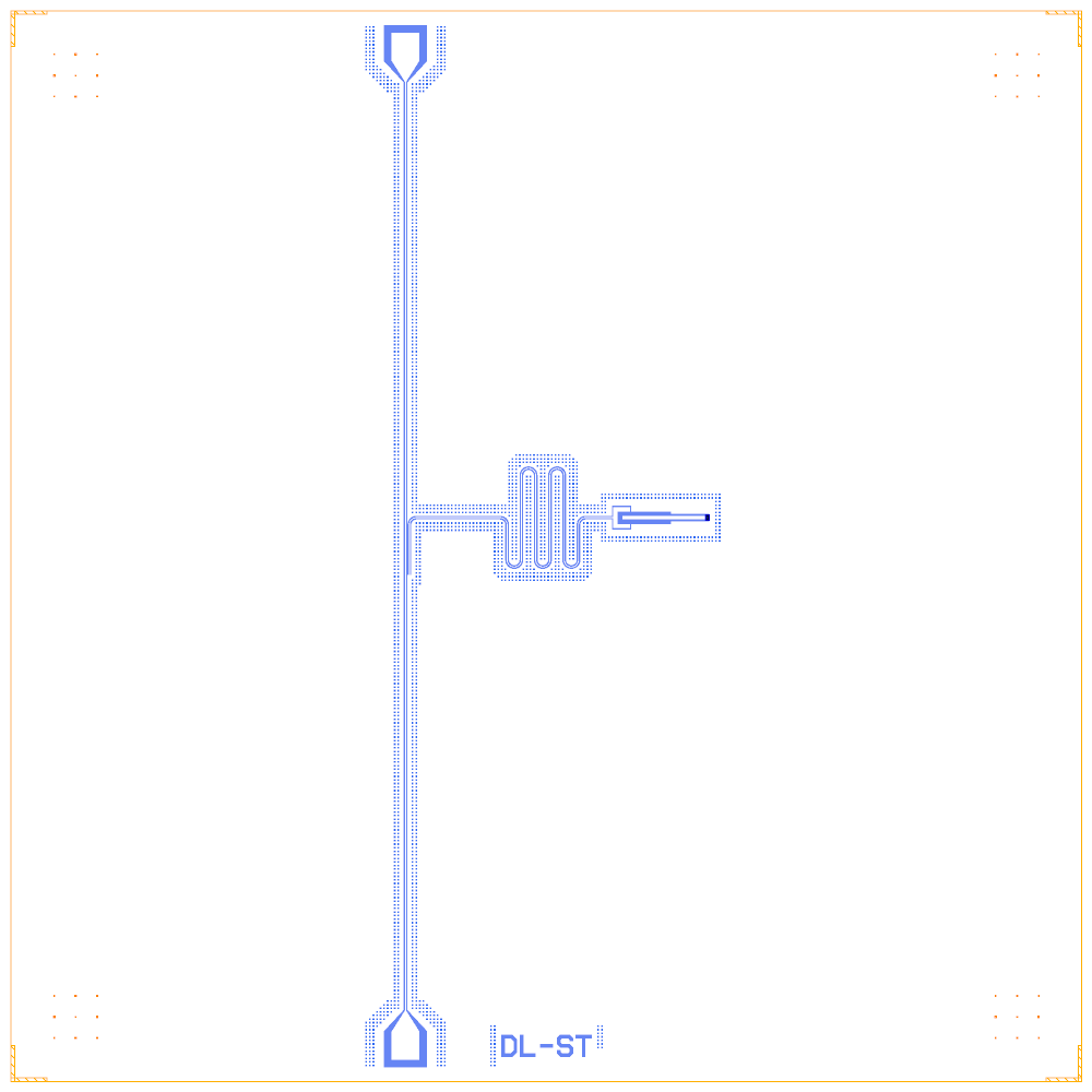
At a glance
Notebook |
|
Source |
DeviceLayout.jl |
Chip |
7.5 × 7.5 mm Quantcore die (the source’s domain is 4 × 3.7 mm), sapphire 650 µm |
On the chip |
1 Swissmon qubit · 1 λ/4 readout · 1 feedline · 2 bond pads |
Builds today |
yes (layout built on 2026-11-19 in 4 s) |
How the notebook builds it
Each Design segment is one cell with a picture of the chip so far (see the notebook template).
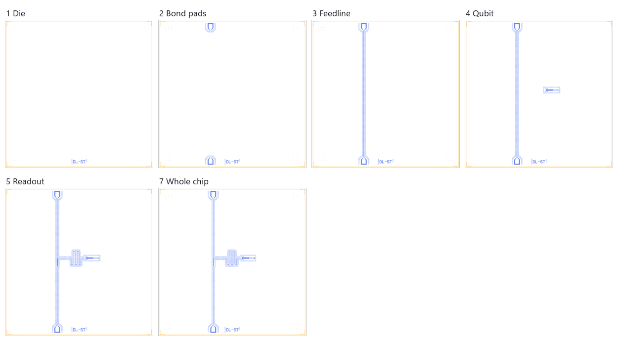
Die. The 7.5 mm die around the source’s simulation domain, with the QCT frame.
Bond pads. Two small pads that end the feedline (the source has lumped ports there).
Feedline. A straight 10 / 6 µm line between the pads.
Qubit. The Swissmon island and the junction sized for 4.05 GHz.
Readout. The clawed λ/4 resonator, hung on the feedline with a 5 µm ground strip.
Coupling. None: there is one qubit.
Routing. None: the source qubit has no drive or flux line.
Whole chip. The Palace targets, the sim group, centring and the save.
LOM estimates
Numbers are from a run of this notebook on 2026-11-19 (Setup, Design, Check and the LOM cells, 6 s): QuCat normal modes with QuTiP dressed values.
mode |
kind |
f (GHz) |
κ (MHz) |
A (MHz) |
participation |
|---|---|---|---|---|---|
Q |
qubit |
4.373 |
0.000122 |
258 |
J_Q 1.00 |
R |
resonator |
5.684 |
0.224 |
0 |
R 1.00 |
parameter |
LOM (QuTiP) |
target |
|---|---|---|
|
4.1 |
3.37 |
|
-307 |
– |
|
-0.708 |
– |
|
5.68 |
5.24 |
|
0.224 |
– |
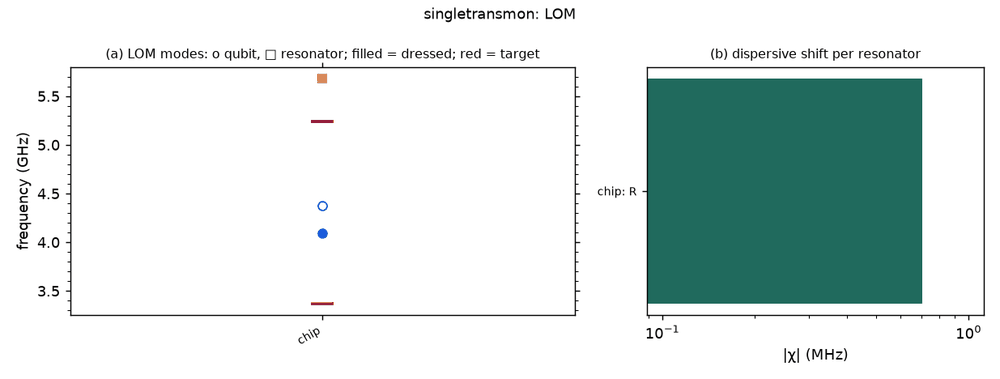
These are lumped-model estimates (component formulas and calibration), not FEM results. The LOM page says how far to trust them.
Build spec
The rest of this page is the detailed spec the notebook was built from, with every component, port, route and length.
Source: examples/SingleTransmon/SingleTransmon.jl
and docs page docs/src/examples/singletransmon.md (rendered)
· components from src/schematics/ExamplePDK (ExampleRectangleTransmon, ExampleClawedMeanderReadout) · licence
MIT (“Copyright Amazon.com, Inc. or its affiliates”, LICENSE.md, verified) · Read on 2026-11-02 (Julia, not run).
What it is: a grounded rectangular transmon island read out by a λ/4 meander. The meander is shorted at its coupled
section, which runs 400 µm alongside a straight 2700 µm feedline, and ends in a claw that wraps the island. Built as a
Palace eigenmode model: lumped ports at both feedline ends, airbridges every 300 µm.
Frame: the simulation domain is 4.0 × 3.7 mm (substrate_x, substrate_y), centred on the floorplan. The feedline
runs vertically (α0 = 90°) from (0, 0) to (0, 2700) in the source, with the resonator on its right (+x). Our estimated
floorplan centre is (1130, 1350), so box (0, 0, 4000, 3700) and Designer ≈ source + (870, 500). The
feedline is then at x 870, y 500…3200. Substrate: sapphire (Palace config εr 9.3/9.3/11.5, tan δ 3e-5/8.6e-5).
CPW 10/6 µm, bend radius 50 µm.
A Swissmon stands in for the rectangle island (Swissmon has a LOM model).
Components
instance |
catalog ref |
key params (units) |
at (x, y) Designer |
rot |
notes |
|---|---|---|---|---|---|
P_S / P_N |
|
the source has no pads, only lumped ports at the line ends |
(870, 300) / (870, 3400) |
0 (faces N) / 180 (faces S) |
or keep the box and accept pads overlapping the domain edge |
Q |
|
island 24 × 620 µm (cap_width × cap_length), cap_gap 30, junction_gap 12. Swissmon: arm_length [12, 298, 12, 298] (WNES), arm_width 24, gap_width [30, 30, 30, 12] |
≈ (2685, 1850) |
90 (N arm and claw face the feedline, −x) |
island centre ≈ 1815 µm right of the feedline (estimate ±50) |
(claw) |
Swissmon N coupler |
claw_trace 34 → cpl_width 34, claw_length 121 → cpl_length 121, claw_gap 6 → cpl_b 6, grasp_width 84 → cpl_gap 84, shield_width 2 |
on Q.cplr1 |
— |
|
Junction: lumped element in Palace, Lj = 14.860 nH, C = 5.5 fF, so junction={"Lj_nH": 14.86, "Cj_fF": 5.5}.
Routes
route |
from → to |
type, length |
hanger |
notes |
|---|---|---|---|---|
FL |
P_S.a → P_N.a |
cpw 10/6 |
straight x 870 (2700 µm between the source port positions) |
|
R |
Q.cplr1 → FL.hanger |
meander 5000 |
s = midpoint (y 1850, i.e. s ≈ 1350 + pad offset), length 400, side right (+x when travelling +y), ground_gap 5 |
λ/4. Short at the far end of the coupled section, then a 500 µm |
Total y extent from the feedline to the claw hook:
428 + 5 + 11 + 500 + (3 + 2·5)·50 = 1594 µm. Airbridges: add_bridges!(…, spacing=300 µm) on all paths, so use
airbridges= on FL and R.
Launchers, pads, test structures, markers, labels
None in the source (lumped ports only). Optional wave-port variant: readout length 4 mm, touching the domain boundary.
LOM node structure
Q: grounded island (C_Σ + Lj 14.86 nH ∥ 5.5 fF to ground) → claw C_g → R (λ/4 CPW, 5000 µm) → coupled-line κ (400 µm, 5 µm ground strip) → FL (two 50 Ω ports). No control lines.
Targets (stated)
Palace eigenmodes with defaults (cap_length 620, total_length 5000): 3.370 GHz (qubit) and 5.244 GHz (resonator). The docs’ optimisation example retargets to [3.0, 4.0] GHz by varying cap_length and total_length, and reaches [3.005, 3.982] GHz.
Simplifications for a first rebuild
Swissmon with short W/E stubs stands in for the rectangular island. A dedicated
ExampleRectangleTransmon(grounded rectangle with end claw) would be exact.Xmonalso works (cross_length 620, but it has a cross).Exact claw shield (2 µm ground shield between claw and island pocket) is optional.
Pads are not in the source. With the 3.7 mm box, use small pads or
launchers=Noneand treat the line ends as ports in simulation.
Build
The notebook is examples/designs/devicelayout/singletransmon.ipynb. It uses the Swissmon stand-in (arm_length [12, 298, 12, 298], N-arm claw 121/34/84). Island at (2685, 2050), coupled section y 1650–2050 (s 1350, backward, short at the south end). Airbridges omitted: KQC auto bridges landed on the neighbouring coupled line. LOM 4.51 / 5.78 GHz vs Palace 3.370 / 5.244 GHz.
Quantcore PDK rebuild
The notebook is a Quantcore PDK rebuild, not a replica: the netlist, LOM and imported components are kept, the process is Quantcore’s.
Notebook: examples/designs/devicelayout/singletransmon.ipynb.
Chip: the Quantcore die frame (L dicing markers 1000/0, 3 × 3 alignment grids 1001/0, chip boundary 100/0, device ID where an edge is free; any brand text is QCT), on the 7.5 × 7.5 mm Quantcore die; the source’s 4 × 3.7 mm Palace domain is centred in it (
box=(-1750, -1900, 5750, 5600)), so every coordinate stays the source’s.Stack: sapphire 650 µm, εr 10.25 (the PDK default stack, used by the LOM estimates and every FEM export); the Palace model uses sapphire with εr 9.3 / 9.3 / 11.5.
Junctions: Quantcore Nb/AlOx/Nb trilayer junctions (
junction_typefromlayouts.registry.trilayer_junction): fingers on 2/0 + 4/0, spacer 50/0 with the 51–53/0 gradient, sized on the PDK junction rule (Nb Δ = 1.4 meV, I_c·R_n = πΔ/2e, R_n·A 13.5 kΩ·µm² and C_J 50 fF/µm² assumed). A single junction, as in the source. Its target f_q 3.37 GHz is below the PDK band (4–8 GHz), so the junction is sized for 4.05 GHz with the LOM C_Σ of the first build (≈ 70 fF): straight finger 0.19 µm (KQC’sjunction_width) × 0.6 µm, L_J ≈ 17.7 nH, C_J ≈ 5.7 fF, so R_n ≈ 121 kΩ, above the 40–50 kΩ window (a 45 kΩ junction would put it at ≈ 6.4 GHz, above the 5.24 GHz readout). The targets stay the source’s.Kept: the topology (rectangle island, clawed λ/4, straight feedline), the 5000 µm readout with its 400 µm coupled section, the claw and island geometry, the targets, the sim group.