Wallraff two-qubit cell (Metal 54)
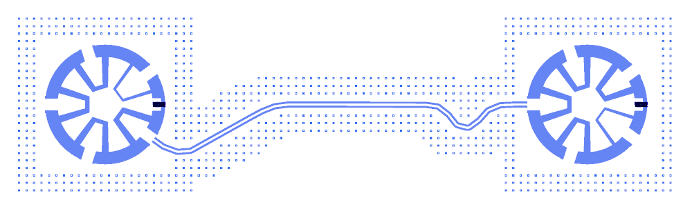
A two-qubit cut-out (data qubit D5 and auxiliary qubit Z3) of the ETH 17-qubit surface-code chip, joined by their coupler line and cropped to the qubits plus a 350 µm margin. It is the Qiskit Metal “54” example (Apache-2.0, © Qiskit Metal contributors), built from the traced layout of notebook 53 after Krinner et al. (Nature 605, 669, 2022). It is a mock-up rather than a mask. The source meshes it for an Elmer capacitance matrix. The Quantcore rebuild is distributed under GPL-3.0.
Build this one to see a small piece of the 17-qubit chip you can mesh and simulate quickly: two star-shaped transmons and a 1.35 mm coupler line. It has no pads, readout or control lines.
At a glance
Notebook |
|
Source |
Qiskit Metal |
Chip |
a 2.3 × 0.7 mm cut-out centred on the 7.5 mm Quantcore die |
On the chip |
2 star transmons (D5, Z3) · 1 coupler line (1349.7 µm, 8.5 / 5.5 µm CPW) |
Builds today |
yes (layout built on 2026-11-19 in 6 s) |
How the notebook builds it
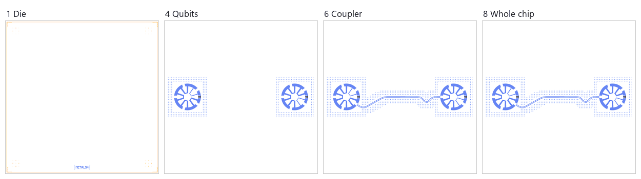
Die. The 7.5 mm die with the QCT frame, the cut-out centred in it.
Bond pads. None: a meshing cut-out has no launchpads.
Readout line. None: the cut-out stops before any readout structure.
Qubits. Two
StarQubittransmons with Quantcore junctions; their readout pads are grounded.Readout resonators. None.
Coupling. The coupler line from D5 to Z3 on the builder’s traced points.
Control lines. None.
Whole chip. The sim group
cell(both qubits and the coupler) for a Q3D C-matrix job, the content centred in the die, the design saved.
LOM estimates
Numbers are from a run of this notebook on 2026-11-19 (Setup, Design, Check and the LOM cells, 6 s): QuCat normal modes with QuTiP dressed values.
quantity |
LOM estimate (fF) |
Elmer, source (fF) |
|---|---|---|
C_Σ D5 |
104 |
167 |
C |
15 |
18.4 |
C_Σ Z3 |
104 |
168 |
C |
15 |
18.4 |
group |
pair |
ZZ (kHz) |
neighbours |
hybridised |
|---|---|---|---|---|
cell |
D5-Z3 |
– |
yes |
yes |
cell |
D5-Z3 |
– |
yes |
yes |
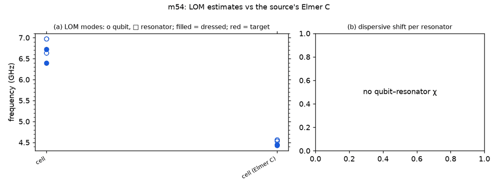
These are lumped-model estimates from component formulas and calibration, not FEM results. The LOM page says how far to trust them.
Build spec
The rest of this page is the detailed spec the notebook was built from: every component, port, route and length.
The
metal:references in this spec build as written, through themetal:wrapper (ports are the Metal pin names, parameters the Metal options).metal:StarQubitresolves (pinspin_cpl1..4,pin_rdout). The Quantcore and KQC substitutions are optional.
Source: Quantum Metal docs/circuit-examples/F.Small-quantum-chips/54-Wallraff_TwoQubit_Cell_Mesh.ipynb, which calls
wallraff_17q.build_cell(("D5", "Z3"), margin=0.35) from resources/wallraff_17q/. Licence Apache-2.0.
The cell is data qubit D5, auxiliary qubit Z3 and the lattice coupler between them, built with exactly the
geometry of 53_wallraff_17q. It is a MultiPlanar design cropped for gmsh + ElmerFEM capacitance (junctions
skipped). Mesh: min 5 µm, max 80 µm.
Chip = the qubits’ bounding box plus a 350 µm margin: 2309.2 × 700 µm. In Metal the chip is centred at (804.6, 0) µm
with D5 at the origin, so Designer = Metal + (350, 350).
The build needs metal:StarQubit.
Components
instance |
catalog ref |
key params (µm) |
at (x, y) |
rot |
notes |
|---|---|---|---|---|---|
D5 |
metal:StarQubit |
radius 160, center_radius 53, gap_couplers 13, gap_readout 6, connector_length 40, trap_offset 11, junc_h 53, 4 connectors, resolution 16 |
(350, 350) |
— |
flux axis A = 0, side s = +1: junction 0°, readout 36°, couplers E 324°, N 108°, W 180°, S 252° (Metal |
Z3 |
metal:StarQubit |
same |
(1959.2, 350) |
— |
A = 0, s = −1: junction 0°, readout 324°, couplers E 36°, N 108°, W 180°, S 252° |
The pads without a line (D5: N, W, S and readout; Z3: E, N, S and readout) reach the pocket edge in the Elmer model, so they become part of ground.
Routes
route |
from → to |
type, length |
waypoints |
notes |
|---|---|---|---|---|
CPL_D5_Z3 |
D5.pin_cpl1 (E neighbour, pad at 324°) → Z3.pin_cpl3 (W neighbour, pad at 180°) |
traced cpw ≈ 1487 µm, 8.5/5.5 |
|
leaves each pin straight for 40 µm. The D5 end leaves 36° below the bond axis (the flux side) and jogs back. Fillet 15 µm, min segment 30 µm |
Launchers, pads, test structures, markers, labels
None. This is a simulation cut-out with no launchpads.
LOM node structure
Two transmon islands (D5_circle_inner, Z3_circle_inner), each with C_Σ to ground. The coupler net (the line plus
the two pads it joins, named Z3_contact_cpl3 by the renderer) carries C to both islands. That gives a 3-node
C-matrix plus the ground reference (Elmer fills the ground diagonal with a placeholder 300 fF). The JJs are added
afterwards as lumped L. Outputs: E_C = e²/2C_Σ per qubit and C(island, coupler). The values are not a full-chip
prediction, because on the chip the free pads connect to resonators and couplers.
Targets (if stated)
None. The notebook prints C_Σ, E_C and the coupler C from the Elmer run; the values are not given in the source text.
Simplifications for a first rebuild
This is a good first test for
metal:StarQubitand for the Designer ↔ LOM C-matrix path. Build it with asim_groupholding both qubits and the coupler route, analysesq3d_cmatrix, margin 0.A geometry-only stand-in is two KQC
CircularTransmonSingleIslandcells (coupler ports at −20/60/−150°) joined by a straight cpw. It is only for testing the meshing pipeline and does not replacemetal:StarQubit.Any other neighbour pair can be built the same way (e.g. X3–D8). Its pad angles follow the rule in the 53 spec.
Quantcore PDK rebuild
The notebook is a Quantcore PDK rebuild of the source, not a replica: the netlist, LOM and imported components are kept, and the process is Quantcore’s.
Notebook: examples/designs/metal/m54_wallraff_cell.ipynb.
Chip: the Quantcore die frame (L dicing markers 1000/0, 3 × 3 alignment grids 1001/0, chip boundary 100/0, device ID where an edge is free; any brand text is QCT), on the 7.5 × 7.5 mm Quantcore die; the source’s 2.3092 × 0.7 mm chip area is centred in it (
box=(-2595.4, -3400, 4904.6, 4100)), so every coordinate stays the source’s.Stack: sapphire 650 µm, εr 10.25 (the PDK default stack, used by the LOM estimates and every FEM export); Metal’s
DesignPlanardefault is silicon (εr 11.45, 750 µm), so the LOM capacitances, resonator frequencies and FEM jobs here are for sapphire rather than the source’s substrate.Junctions: Quantcore Nb/AlOx/Nb trilayer junctions (
junction_typefromlayouts.registry.trilayer_junction): fingers on 2/0 + 4/0, spacer 50/0 with the 51–53/0 gradient, sized on the PDK junction rule (Nb Δ = 1.4 meV, I_c·R_n = πΔ/2e, R_n·A 13.5 kΩ·µm² and C_J 50 fF/µm² assumed); bothStarQubits get the PDK nominal junction, 0.5 × 0.6 µm fingers → R_n = 45 kΩ, L_J = 6.73 nH, C_J = 15 fF (in the 40–50 kΩ window) (the source skips junctions and computes electrostatics only). Expected f_q ≈ 6.7 / 7.0 GHz from the LOM C_Σ; with the source’s Elmer C-matrix (C_Σ ≈ 167 fF) ≈ 4.6 GHz.Kept: the topology and every Metal component with the source’s options (through the
metal:wrapper), positions and orientations, every route’s end pins and total length, the sim groups (the traced 31-point coupler line, 8.5 / 5.5 µm CPW).