Tutorial 2: IBM bowtie
examples/tutorials/02_ibm_bowtie_5q.ipynb builds IBM’s first cloud processor, the five-qubit “bowtie” (ibmqx2
Yorktown and ibmqx4 Tenerife), from its published device data. There is no public layout of this chip: the topology and
the targets come from IBM’s data, and the layout is ours. The tutorial follows the design notebook
examples/designs/ibm/ibm_bowtie_5q.ipynb step by step (spec: IBM bowtie 5q).
New in this tutorial: pocket transmons, λ/2 buses with tees, J by avoided crossing, and a FEM stage that simulates only
one qubit of the five.
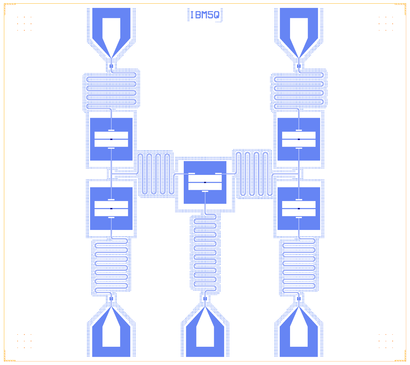
Section 5: the whole chip. Two buses join the qubits through tees; each qubit has its own readout line.
What the chip is
Five fixed-frequency transmons and two bus resonators. Each bus couples three qubits (Q0, Q1, Q2 on one; Q2, Q3, Q4 on the other), so the coupling graph is two triangles sharing Q2: the bowtie. Each qubit has its own readout resonator and line.
From IBM’s data |
Here |
|
|---|---|---|
Topology |
Coupling map 0-1, 0-2, 1-2, 2-3, 2-4, 3-4 |
Each bus is a λ/2 line from Q2 to a tee whose two stubs reach the other two qubits |
Qubits |
Floating two-pad transmons |
Quantum Metal |
f_q, α, J |
f_q 5.03 to 5.29 GHz, α -330 to -376 MHz, J 1.2 to 2.0 MHz |
f_q matched per qubit by its junction; α about -145 MHz |
Buses, readouts |
Buses 7.0 and 6.6 GHz; readouts 6.44 to 6.58 GHz |
The same targets; λ/2 readouts through a series finger capacitor to a 50 Ω pad |
The licence note is in the notebook: IBM’s device values come from the Qiskit FakeYorktown data (Apache-2.0) and the
ibmqx4 bus frequencies from arXiv:1805.10478.
The sections
Section |
What it does |
What comes out |
|---|---|---|
1 Targets and junctions |
Device data become targets; |
A table of asked and drawn L_J (6.09 to 6.63 nH asked), C_J and R_n 40.9 to 44.1 kΩ |
2 Die and floorplan |
A 9 × 8 mm die, device ID |
The empty die; Q0/Q1 left, Q3/Q4 right, above and below the bus height |
3 Pads |
One |
All five pads at 100.0 µm from the die edge |
4 Components |
Five pocket transmons and two |
The pocket pad width sets the coupling: 150 µm on the buses (J), 140 µm on the readouts |
5 Routes |
Two λ/2 buses with meanders and stubs, five λ/2 readouts |
Route lengths (BusA 8190 µm, BusB 8750 µm, readouts 9348 to 9562 µm) and the chip picture |
6 DRC |
Errors, warnings, PDK report |
0 errors, 10 warnings (all |
7 Netlist and LOM |
The left triangle as a netlist |
22 nodes and 80 branches for the whole chip |
8 LOM against IBM |
Each qubit with its readout chain; each triangle; J by avoided crossing |
Tables of f_q, α, f_r, κ, χ, the bus modes and J |
9 FEM stage 1 |
Sim groups, the subset |
Convergence, C-matrix, eigenmode, filled capacitances |
10 FEM stage 2 |
The subset values in the whole netlist; feedback |
LOM versus FEM; a revision with new L_J and lengths |
11 Iterate |
Widen Q0’s bus pad from 150 to 200 µm |
J(Q0-Q2) changes |
12 Build and export |
|
Fab layer table |
13 Snapshots |
The triangle, the junction, a finger capacitor, the fab view |
Pictures |
14 Summary |
What matches the source, what differs |
A table |
3 to 5: the layout
TransmonPocket6 is a floating two-pad transmon in a ground pocket (island1, island2) with the junction across the
20 µm pad gap. Connection pads are named and placed by loc_W and loc_H; Q2 has two bus pads (bw, be) and a
readout pad ro, the outer qubits have bus and ro. A small helper, cpad(name, loc_w, loc_h, width), builds the
connection-pad dictionary.
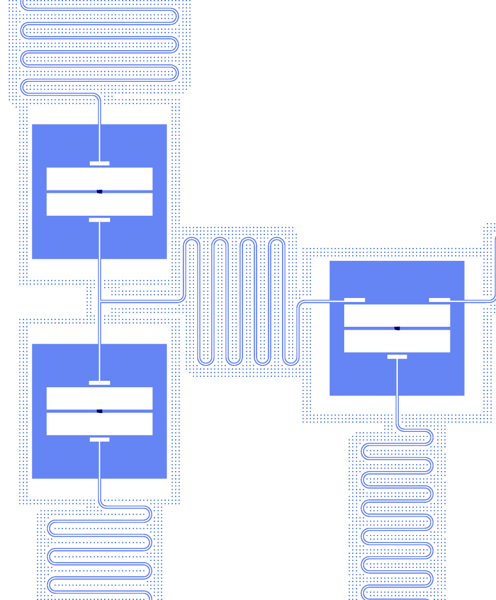
Section 13: the left triangle. Two pockets, the tee and its stubs, the bus meander and Q2.
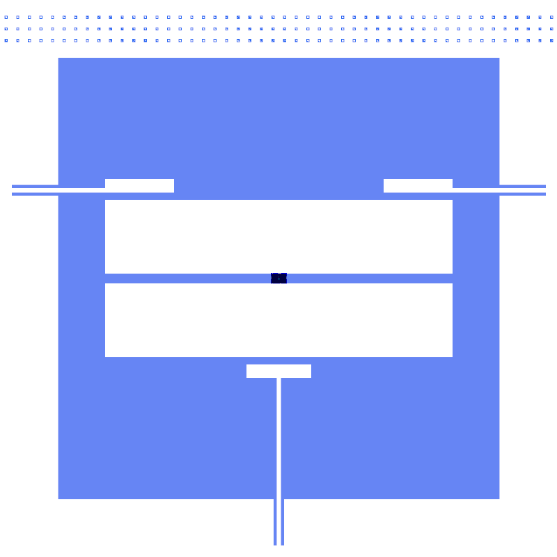
Q2’s pocket transmon: the two bus pads at the top, the readout pad at the bottom and the trilayer junction across the pad gap.
Each bus is a meander from Q2’s bus pad to the tee’s second_end (λ/2 for 7.0 and 6.6 GHz, both ends at a voltage
antinode), then two straight stubs from the tee to the outer qubits. One waypoint keeps each bus meander in the channel
between the pockets. The readouts are meanders from each ro pad to its finger capacitor, then a 50 Ω line to the
bond pad.
8: LOM against IBM
Each qubit with its readout chain (λ/2, finger capacitor, pad line, 50 Ω port), IBM’s values in brackets:
Qubit |
f_q (GHz) |
α (MHz) |
Readout f_r (GHz) |
κ (MHz) |
χ (MHz) |
|---|---|---|---|---|---|
Q0 |
5.2684 (5.2823) |
-145.1 (-330.8) |
6.429 (6.5304) |
0.908 |
-0.888 |
Q1 |
5.2244 (5.2475) |
-145.5 (-330.4) |
6.3808 (6.4817) |
0.888 |
-0.878 |
Q2 |
5.028 (5.0334) |
-143.2 (-376.1) |
6.3367 (6.4365) |
0.871 |
-0.737 |
Q3 |
5.2685 (5.292) |
-145.2 (-329.7) |
6.4765 (6.5789) |
0.929 |
-0.841 |
Q4 |
5.0893 (5.0785) |
-147 (-333.1) |
6.4285 (6.5301) |
0.909 |
-0.687 |
f_q and f_r land on the targets. α does not: it comes out near -145 MHz, not IBM’s -330 MHz. The PDK junction window (R_n 40 to 50 kΩ) caps L_J at about 7.5 nH; at the same f_q that means a larger C_Σ, hence a smaller |α| (about E_C). The limit comes from the PDK; the layout is not the cause.
Each triangle as one circuit gives the bus mode (BusA 6.9110 GHz, BusB 6.5112 GHz, targets 7.0 and 6.6) and the three
qubits. J of a pair is half the minimum splitting at the avoided crossing, found by sweeping the second qubit’s L_J
through the first’s frequency (C.exchange_coupling):
Pair |
J (MHz) |
Target J (MHz) |
ZZ (kHz) |
|---|---|---|---|
Q0-Q2 |
1.61 |
1.82 |
-30 |
Q1-Q2 |
1.55 |
1.24 |
-63.1 |
Q2-Q3 |
1.56 |
1.82 |
-45.9 |
Q2-Q4 |
1.57 |
1.81 |
69.6 |
J lands at IBM’s 1.2 to 2.0 MHz scale. The Q0-Q1 and Q3-Q4 pairs need the whole triangle (about 2 minutes each), so
they are off by default; set ALL_PAIRS = True to include them. These tables are component estimates, simulated circuit
by circuit because QuCat on all five qubits and seven resonators at once takes more than 10 minutes.
9 and 10: FEM
SIM_SUBSET = [("Q2", None)] is the default: None means the qubit’s own readout chain. The box holds Q2 with its
readout, its finger capacitor and the line to the pad; BusA and BusB are cut at the qubit. Two jobs run: Q3D and a
qubit-only eigenmode (SUBSET_ANALYSES). The kept results:
Job |
Passes |
Last Δ / target |
Converged |
Wall time |
|---|---|---|---|---|
|
7 |
1.99 / 2.0 % |
no |
54.6 s |
|
2 |
1.41 / 1.0 % |
no |
218.3 s |
The eigenmode gives Q2’s dressed f_q of 5.0963 GHz and α of -145.3 MHz (p_J 0.9923). The Q3D run filled 12 branches of the netlist; 51 keep their estimates. The LOM on the filled netlist moves Q2’s f_q from 5.028 to 5.235 GHz and its readout χ from -0.7369 to -1.172 MHz; the pyEPR value is 5.096 GHz (-2.6 % against the filled LOM). Both buses move up by about 1.6 %: BusA 6.91 to 7.029 GHz (target 7.0), BusB 6.51 to 6.617 GHz (target 6.6).
The notebook then renders the Q2_read group into AEDT without solving it (hfss.render(..., solve=False), about
30 s) and reads the project back with hfss.check_project. The kept check reports “rendered in 16.0 s; 10 boundaries,
7 nets; OK”: design type, the sapphire stack, 9 of 9 metal sheets, every net named after its LOM node. It checks cheaply
that the geometry reaches AEDT before a solve that takes hours.
Feedback moves each component’s own knob, because loop.feedback’s surrogate knows the Xmon knobs but not the pocket
transmon’s. L_J scales as (f_q / target)² and each λ/2 length as f / target:
Component |
f_q → target (GHz) |
L_J (nH) |
Readout λ/2 (µm) |
|---|---|---|---|
Q0 |
5.2684 → 5.2823 |
6.090 → 6.058 |
9420 → 9274 |
Q2 |
5.2346 → 5.0334 |
6.590 → 7.127 |
9562 → 9584 |
BusA |
7.0289 → 7.0 |
8190 → 8224 |
|
BusB |
6.6172 → 6.6 |
8750 → 8773 |
The notebook shows all seven rows. The revision examples/tutorials/designs/t02_ibm_bowtie_5q_fb.json is DRC clean,
and the notebook writes its fab file. The consensus on the whole netlist reports 1 of 15 targets within tolerance.
FEM_WHOLE = True is opt-in. It solves the built-in group chip (nothing cut, a 50 Ω port on each pad). The whole-chip
Q3D takes about 3 minutes (180 s) and a few GB. The eigenmode and driven runs of the whole chip were not run: one
9.5 mm λ/2 box alone took 197 000 tets and 10.8 GB, and the whole chip would need over 30 GB and hours.
11: iterate
Widening Q0’s bus pad from 150 to 200 µm on a copy of the design:
Quantity |
Before |
After |
Change |
|---|---|---|---|
J(Q0-Q2) (MHz) |
1.6145 |
2.0257 |
+25.5 % |
f_Q0 (GHz) |
5.2675 |
5.2408 |
-0.5 % |
f_Q2 (GHz) |
5.0315 |
5.0315 |
0 |
The DRC stays clean. The bus pad width is the geometry knob for J.
12: export
export_fab writes the PDK fab layers with the build’s cheese (11106 holes, the PDK band: the source has none) and
rounded corners. This chip has no airbridges. CLI: qcc build, qcc design drc, and qcc sim build ... -g triangle_A -a q3d_cmatrix.
Pitfalls
α is -145 MHz rather than -330 MHz because of the PDK junction window. It is not a bug.
squid_aandsquid_bwarnings are junction attachment points (the junction is drawn by the cell).Where a box edge cuts a bend, the 50 Ω port gets no polygon and the builder prints
Unable to create polygon for port ...warnings. The notebook output shows four of them while it exports the groups. Check that the cut sits on a straight section.The pair loop for Q0-Q1 and Q3-Q4 is off by default (
ALL_PAIRS = False).A stage-2 LOM on a subset leaves most branches on estimates (the table says “estimate (not simulated)”). Do not read a 0.0 % change on those rows as agreement.
Tutorial 3 scales this up to 17 qubits.