Tutorial 3: Surface 17
examples/tutorials/03_surface17.ipynb builds two 17-qubit surface-code chips with the same topology from one
generator, examples/designs/devicelayout/_surface17.py. Part A is the DeviceLayout.jl DemoQPU17 (© Amazon.com, Inc.,
MIT licence). Part B is the ETH Zurich 17-qubit device (Krinner et al., Nature 605, 669, 2022; arXiv:2112.03708), with
the targets from the paper’s Table I and the layout mock-up from Quantum Metal notebook 53. This is the biggest chip in
the tutorials. A generator replaces hand-placed cells, crossings become airbridges, and the chip is simulated one qubit
group at a time because it is too large to solve whole. The specs are DemoQPU17 and the
design groups.
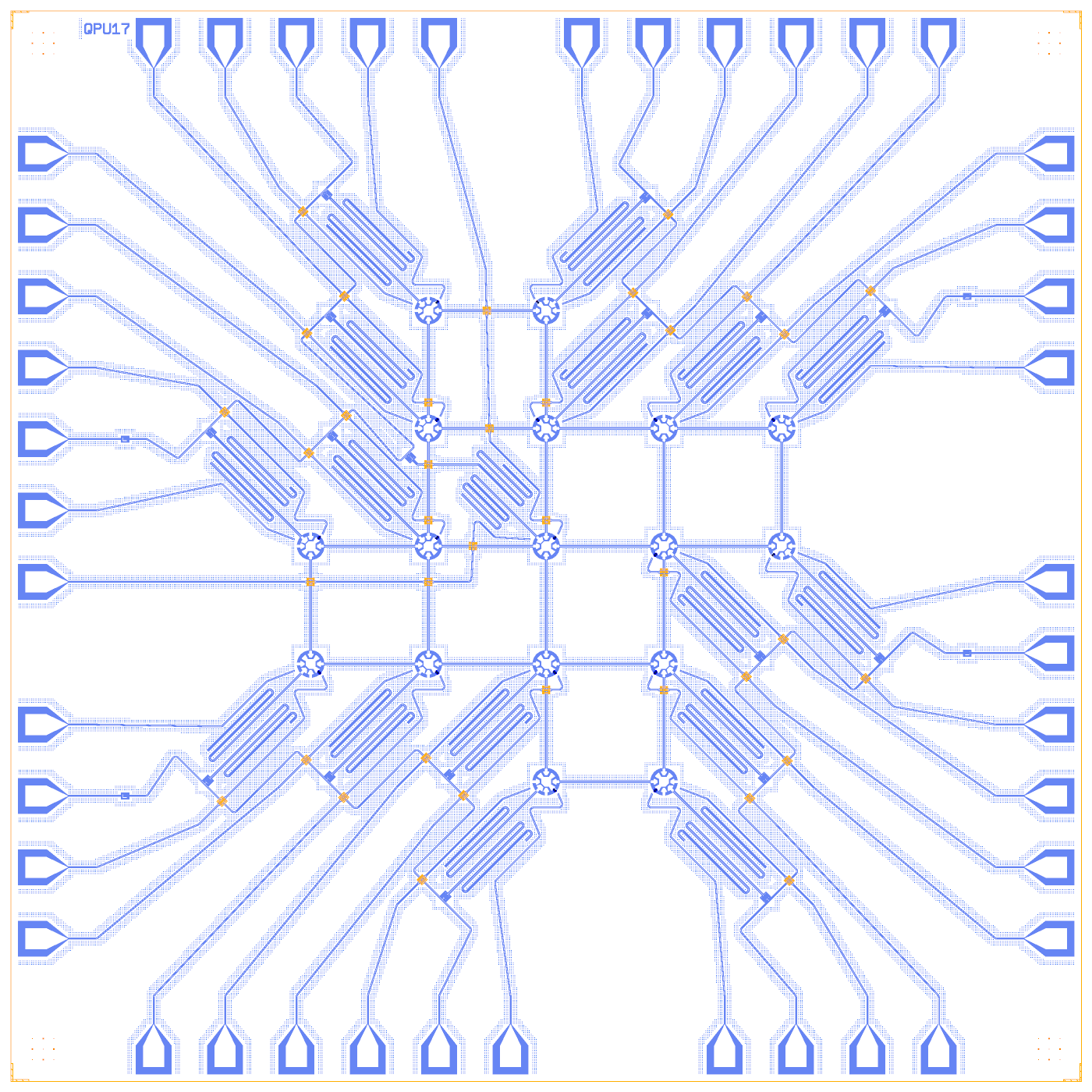
Part A, section A7: DemoQPU17 with couplers, readout modules, feedlines and control lines.
What the chip is
Idea |
What it means here |
|---|---|
The lattice |
17 transmons on a 5 × 5 grid: 9 data and 8 auxiliary (measure) qubits in a checkerboard, and 24 nearest-neighbour CPW couplers |
Readout with Purcell filters |
Each qubit has a λ/4 readout resonator tapped to its own λ/4 Purcell filter. Only the filter touches the feedline (through a capacitive tee). Four feedlines read 4 or 5 qubits each, each with an input capacitor |
Control lines |
An XY (drive) and a Z (flux) line per qubit: 34 lines from the pads into the lattice |
Crossings and airbridges |
The generator finds every crossing and splits the higher-ranked line there; an |
What the PDK changes: StarQubit (a Quantum Metal five-pad transmon) with a trilayer SQUID, pads 100 µm from the die
edge, the QCT frame and the PDK cheese band.
The sections of part A
Section |
What it does |
What comes out |
|---|---|---|
A1 The lattice |
|
A text grid of the 17 sites (d = data, a = auxiliary) and 24 couplers |
A2 What the source fixes |
Port map, readout targets, feedline groups, mirroring |
A table of the four feedlines (for example feedline 1 runs from port 44 to 3 through Q31, Q32, Q33, Q22, Q12) |
A3 Floorplan and plan |
|
The plan: 17 StarQubits, 17 tees, 4 input capacitors, 42 pads, 37 airbridges, 154 routes, 0 problems |
A4 Junctions |
|
A table of L_J, R_n per junction and device R_n; several qubits are outside the 40 to 50 kΩ window |
A5 Die and pads |
42 pads |
Every pad at 100.0 µm from the die edge |
A6 Components |
17 |
A picture of Q33 |
A7 Routes |
Couplers, readout modules, feedlines, Z then XY lines |
117 instances, 154 routes, nothing left unplaced |
A8 DRC |
0 errors, 54 warnings, 12 PDK design warnings |
|
A9 Netlist and LOM |
The 17-qubit node structure |
138 nodes, 351 branches (250 C, 42 R, 42 |
A10 LOM against targets |
Each qubit with its readout chain and its whole feedline |
A table of f_q, α, f_r, κ, χ for readout and filter; a coupled pair |
A11 FEM |
Stage 1 on |
Convergence, C-matrix, builder notes |
A12 Iterate |
Q13’s readout gap 8 to 15 µm |
A before/after table |
A13 Build and export |
|
Fab layer table with the airbridge layers |
A14 Snapshots |
The centre plaquette, a module, a SQUID, an airbridge, the fab view |
Pictures |
Part B repeats the steps for the ETH chip, then a summary table covers both.
A1 to A7: plan and build
S17.plan_chip(cfg) lays everything out on paper first: instances, the polylines of every line, the crossings and the
airbridges. The notebook then adds the instances in d.batch() blocks and the lines by rank. The centre qubit Q33 sits
in a closed plaquette (all four neighbours around it), so its readout hairpin is shortened and its tee and Purcell
filter sit in the channel west of the plaquette, with the filter lead bridged over a coupler.
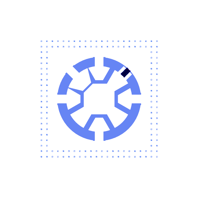
A StarQubit (Q33): the star-shaped island with five pads and the SQUID in the gap between two coupler pads.
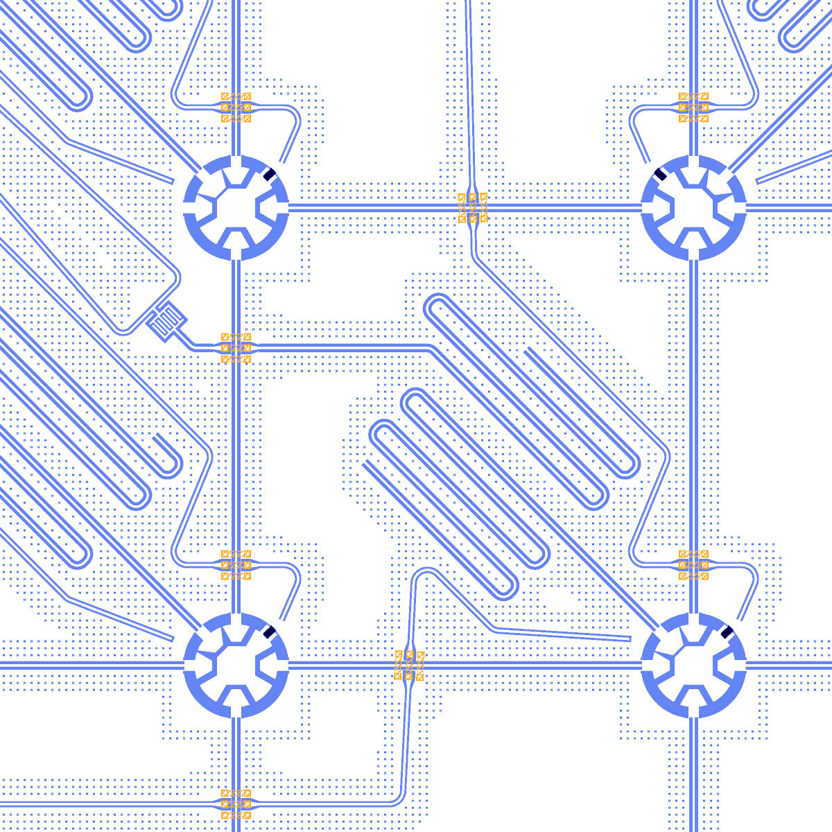
Section A14: the centre plaquette with its bridged crossings.
Readout and Purcell lengths are v_ph / 4f times a loading factor (0.96 and 0.948), calibrated once with the LOM.
A4 to A8: junctions and DRC
The SQUID junctions are sized from the target frequencies. The table lists R_n per junction and for the device: Q13 needs L_J 11.30 nH, which
the table gives as 150.0 kΩ per junction and 75.0 kΩ for the device, outside the 40 to 50 kΩ window. The DRC reports pdk_rn on
those 12 qubits and does not retune them. The 54 warnings are dangling_port: the qubits’ squid_a/b and the 20 coupler
pads of edge qubits with no neighbour on that side.
A9 and A10: LOM
Each qubit is simulated with its readout chain and its whole feedline. The notebook expects f_q within about 5 % of the plan, f_r within 1 to 3 %, the filter resonant with its readout, κ of the filter about 30 MHz and χ of -5 to -15 MHz. Examples from the saved table:
Qubit |
f_q, LOM (plan) GHz |
Readout f_r, LOM (target) GHz |
κ readout (MHz) |
χ (MHz) |
|---|---|---|---|---|
Q31 |
4.8135 (4.95) |
7.1376 (7.2) |
4.97 |
-9.88 |
Q33 |
4.8094 (5) |
6.7664 (6.8) |
4.54 |
-11.9 |
Q12 |
5.5361 (5.8) |
7.02 (7) |
3.16 |
-13.5 |
Q54 |
5.8639 (6.15) |
7.0373 (7) |
1.38 |
-22.9 |
A coupled pair, Q23 and Q33 through their 1.3 mm coupler, gives two qubit modes about 0.9 GHz apart (5.2048 and 6.0664 GHz, no hybridisation) and a static ZZ of -2.064e+04 kHz. That is large because the StarQubit LOM gives every coupler pad the same arc and the coupler route has no line capacitance in the LOM yet (a known LOM request, see the status page).
A11: FEM
A 17-qubit chip does not fit a workstation. Stage 1 solves one qubit and its readout chain (SIM_SUBSET = [("Q23", None)], Q3D only). The groups exported in this notebook are:
Group |
Analysis |
Gives |
|---|---|---|
|
|
The two qubits and their coupler: C_Σ, pad capacitances, g |
|
|
Q12 with its readout hairpin, tee and Purcell hairpin: f, κ, χ |
|
|
Q33’s closed-plaquette module whose filter lead is bridged |
Airbridges are dropped by default in simulation exports (a note flags each crossing, whose line is then open in the FEM
model). airbridges=True, the group setting settings={"airbridges": True} or the CLI --airbridges keeps them; the
notebook exports both variants.
The kept SUB Q3D (8 passes, last Δ 2.69 / 2.0 %, 54.6 s, not converged) fills 0 branches of the netlist. The
StarQubit’s pin stubs get no excitation, because their waveguide ports have no polygon on this 45 degree lattice, so
its coupler and readout pads come out as ground in the C-matrix. fill notices the pins have no net and keeps the
estimates (the “StarQubit pin guard”). So the stage-2 LOM values are still the component estimates:
the table shows 0.0 % change. This is an open issue, and the 0.0 % is not a result.
With RUN_FEM = True, the notebook renders the pair Q23_Q33 (Q3D, no solve) to check that the components reach AEDT
intact. The kept check says “rendered in 20.5 s; 11 boundaries, 5 nets; OK”. FEM_WHOLE = True renders the whole chip
the same way (no solve; its job is ready for a server).
A12: iterate
Q13 is a data qubit with the narrow 8 µm readout gap. Widening it to 15 µm (the auxiliary value):
Quantity |
Before |
After |
Change |
|---|---|---|---|
Q13 f_q (GHz) |
4.6706 |
4.7488 |
+1.7 % |
Q13 α (MHz) |
-223.38 |
-233.24 |
-4.4 % |
RO_Q13 f_r (GHz) |
7.2276 |
7.2884 |
+0.8 % |
RO_Q13 χ (MHz) |
-8.7361 |
-4.1378 |
+52.6 % |
RO_Q13 κ (MHz) |
4.3148 |
13.327 |
+208.9 % |
The pins do not move (they sit at 1.25 times the pocket radius), so every route stays where it is. The DRC stays clean.
A13: export
The fab export keeps the build’s cheese (81776 holes) and rounds corners. The airbridge layers go to 300/0 (pads) and
301/0 (bridges): the report shows 222 AIRBRIDGE_PADS and 111 AIRBRIDGE_BRIDGE polygons.
Part B: the ETH device
The same steps with a different Config: the mock-up’s lattice pitch (1609.2 × 1753.9 µm), the paper’s names (D1 to
D9, X1 to X4, Z1 to Z4), D5 in the closed plaquette and a 180 µm StarQubit so that α lands near the paper’s -164 to
-192 MHz. Here the whole plan is added in one d.batch() through S17.build, then C.pads_to_edge(d) moves all 42
pads to the 100 µm rule (the notebook prints “42 pads moved to 100 µm from the edge”).
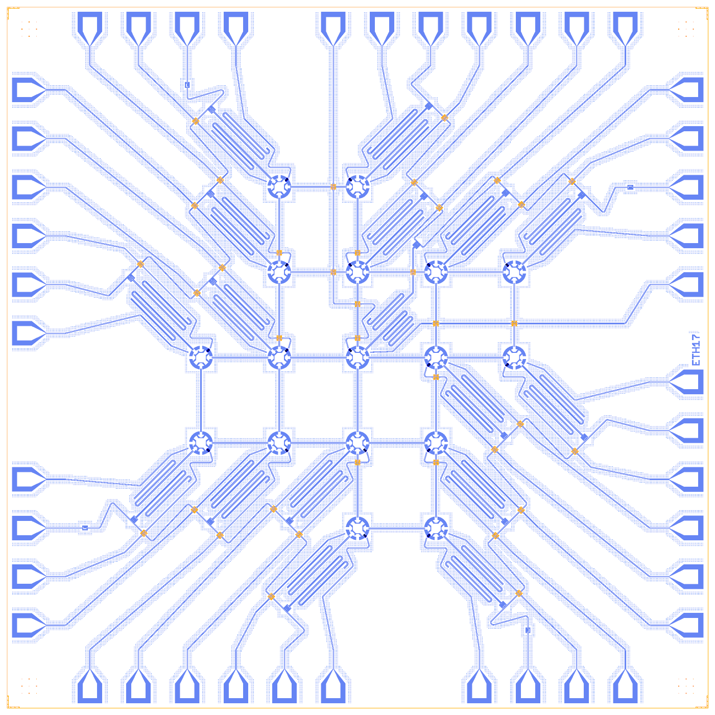
Part B: the ETH 17-qubit device from the same generator.
The DRC gives 0 errors, 54 warnings and 24 PDK design warnings: pdk_rn on 17 qubits and pdk_fq on 7 data qubits,
which the paper idles at 3.74 to 4.14 GHz, below the PDK band of 4 to 8 GHz. They are flagged and kept, since the
targets are the paper’s. The LOM against Table I:
Qubit |
f_q LOM (paper) GHz |
f_r LOM (paper) GHz |
g LOM (paper) MHz |
χ LOM (paper) MHz |
|---|---|---|---|---|
D1 |
3.803 (3.885) |
6.766 (6.769) |
351 (244) |
-2.54 (-2.0) |
D5 |
3.804 (3.895) |
7.155 (7.18) |
392 (238) |
-2.48 (-1.5) |
X2 |
5.856 (5.885) |
7.557 (7.554) |
321 (168) |
-5.75 (-1.9) |
Z1 |
6.220 (6.328) |
7.348 (7.316) |
339 (171) |
-13.84 (-4.7) |
f_q is within about 2 % and f_r within about 0.5 %; g and χ come out above the paper, because the StarQubit LOM’s pad
arcs are rough. The D5_Z3 C-matrix job is meant to calibrate them. The notebook also exports D5_readout
(eigenmode, with D5’s bridged filter lead and airbridges kept) and D5_Z3 (Q3D), and shows the Quantum Metal mock-up’s
own geometry for comparison.
Pitfalls
Several qubits are outside the PDK R_n window (
pdk_rn). The notebook flags and keeps them: the targets come from the source.The LOM of this chip is on estimates (the StarQubit pin guard). Do not read the LOM-versus-FEM table as agreement.
The readout-filter tap is declared (
d.couple, 1.2 fF), not drawn. There are no ground-plane holes or ground airbridges, and the XY and Z lines are not drive and flux controls in the LOM (the StarQubit has no such ports).Simulation exports drop airbridges by default. A feedline crossing is then open in the FEM model.
A box that cuts a line at 45 degrees gets its 50 Ω port on the line’s own axis; the builder lists those ports as notes.
Tutorial 4 closes the design loop on two qubits.