Tutorial 4: Feedback loop
examples/tutorials/04_two_qubit_feedback_loop.ipynb extends tutorial 0 to two Xmons side by
side, coupled through their facing cross arms, each read out by its own λ/4 hanger on one shared feedline. It runs the
design loop as a loop: the chip is a function of ten numbers (the knobs), the LOM and the FEM measure it, and a
feedback step turns the differences into new knobs until the chip lands on its targets. At the end you give a new qubit
frequency and the notebook redesigns, re-simulates and writes the fab layout. The loop itself is described on
the flow page and the feedback page.
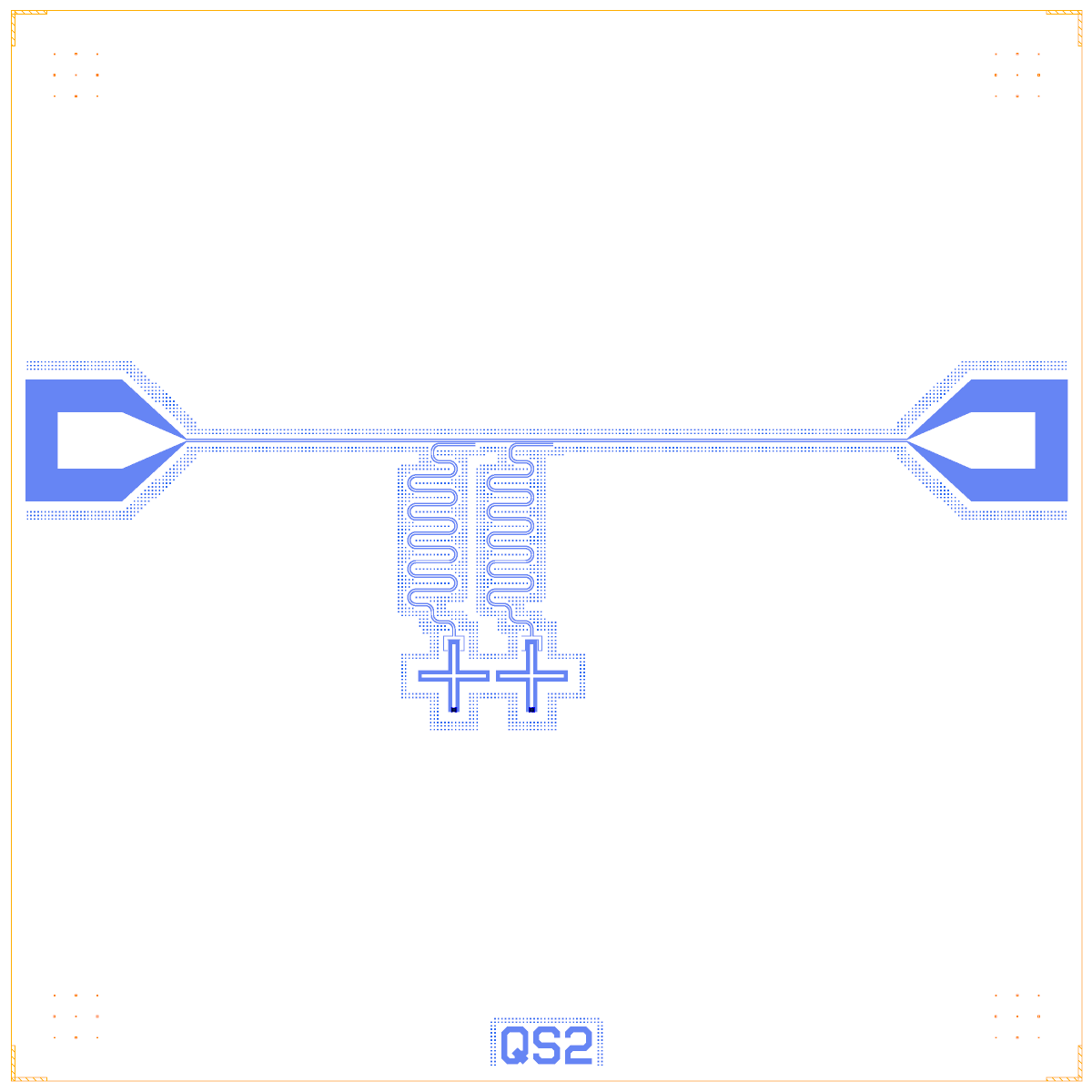
Section 4: the two-qubit chip, with its two pads and feedline.
The targets and the knobs
Five targets, with the tolerances the loop stops on:
Target |
Value |
Tolerance |
Knob that moves it |
Update rule |
|---|---|---|---|---|
|
5.35 |
± 0.005 |
Cross length (and, out of range, the junction within the PDK R_n window) |
L·C ∝ 1/f² |
|
5.65 |
± 0.005 |
Same |
Same |
|
7.00 |
± 0.005 |
The λ/4 meander length |
λ/4 ∝ 1/f |
|
7.30 |
± 0.005 |
Same |
Same |
|
10 |
± 0.3 |
The ground strip between the facing arm tips |
J ∝ C_c |
The ten knobs of design(knobs) are x1, cross1, cross2, lj1, lj2, strip, cpl1, cpl2, len1, len2.
The coupling C_c is a power law of the tip gap, anchored on the last C-matrix.
The sections
Section |
What it does |
What comes out |
|---|---|---|
1 Targets |
The five targets and tolerances, the PDK rules |
Pad edge 100 µm; L_J window 5.99 to 7.48 nH |
2 The design as a function |
|
A reusable function |
3 LOM-first synthesis |
λ/4 lengths from f_r, L_J from C_Σ, the strip from J |
A knob table (revision 0 start) |
4 Build, DRC, netlist |
One build |
DRC clean; 6 nodes, 15 branches; pads at 100.0 µm; pictures |
5 LOM and the LOM loop |
|
Four loop steps, revision 0 saved as |
6 FEM stage 1 |
Two groups, |
Convergence, C-matrix, eigenmodes, S21 notches, filled capacitances |
7 FEM stage 2 |
|
LOM versus FEM table |
8 Feedback |
δ = FEM minus LOM, corrected targets, revision 1 |
New knobs; rev 1 DRC clean |
9 Re-simulate revision 1 |
The same jobs on rev 1 |
A table: target, FEM rev 0, predicted rev 1, FEM rev 1 |
10 “I want f_q1 = X GHz” |
Change |
A new revision, DRC, FEM, residuals |
11 The fab layout |
|
Fab layer table, |
12 Snapshots |
The chip, the tips, a junction, before and after your change |
Pictures |
13 Summary |
A table of every step |
1 to 3: targets and synthesis
No layout is guessed by hand. The readout length is the bare λ/4 for each f_r on the PDK CPW (the claw loads the open
end, so these land low). The junctions come from a first draft at cross 450 µm that gives each island’s C_Σ (99.2
fF); size_junction(f_q, C_Σ) then gives L_J:
Qubit |
C_Σ (fF) |
L_J for f_q (nH) |
R_n (kΩ) |
In the PDK window |
|---|---|---|---|---|
Q1 |
99.2 |
7.354 |
49.1 |
yes |
Q2 |
99.2 |
6.520 |
43.6 |
yes |
The coupling gives C_c = 0.416 fF for J = 10 MHz, which is a strip of 45.7 µm (tip gap 95.7 µm). From then on the cross length tunes f_q continuously, because the drawn L_J only comes in steps of about 2 %.
4 and 5: build and the LOM loop
The first build is DRC clean (0 errors, 0 warnings). The LOM on the synthesised knobs:
Quantity |
Target |
LOM (synthesis) |
|---|---|---|
|
5.35 |
5.3445 |
|
5.65 |
5.6508 |
|
7 |
6.2513 |
|
7.3 |
6.4914 |
|
10 |
9.7311 |
The resonators land about 0.75 GHz low. The loop rebuilds, simulates and updates until everything is inside the tolerances:
Step |
Q1 f_q |
Q2 f_q |
R1 f_r |
R2 f_r |
g (MHz) |
|---|---|---|---|---|---|
0 |
5.3445 |
5.6508 |
6.2513 |
6.4914 |
9.7311 |
1 |
5.3493 |
5.6508 |
6.9156 |
7.2053 |
10.0149 |
2 |
5.3499 |
5.6502 |
6.9905 |
7.2890 |
10.0018 |
3 |
5.3500 |
5.6501 |
6.9989 |
7.2987 |
9.9994 |
This is revision 0: the design the LOM says is on target. The resonator lengths move most (len1 4501 to 3965.9
µm); the qubits and J need small corrections. Each step is a full rebuild, about 10 s.
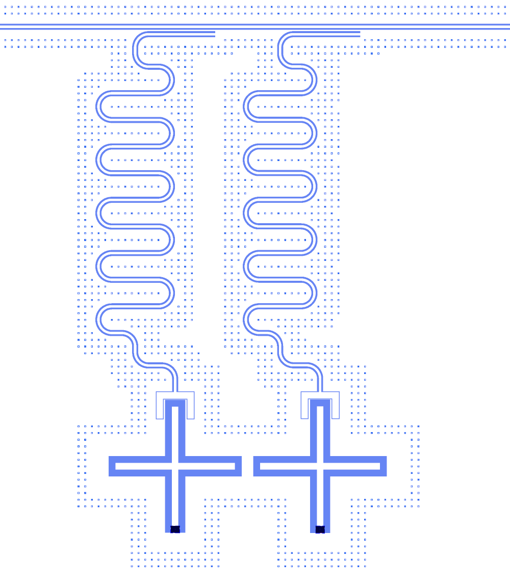
Section 5: revision 0 after the LOM loop, the two qubits with their readouts and the feedline.
6 and 7: FEM
Two sim groups:
Group |
Analyses |
Box |
Gives |
|---|---|---|---|
|
|
Both qubits and 200 µm (about 1.4 × 1.0 mm); R1 and R2 are selected, so the build cuts them at the claws |
C_island, C_g, C_claw of each qubit and the arm-to-arm C_Q1Q2, hence J |
|
|
Both qubits, both readouts and the feedline stretch, plus 150 µm (about 1.4 × 2.2 mm) |
Eigenmode: f_q, α, f_r, χ, κ, ZZ. Driven: two S21 notches |
The eigenmode asks for 5 modes above 4.5 GHz (two qubits, two resonators and a spare slot). The driven run has a 10 µm mesh seed on the gaps. The kept results for revision 0 (fast settings):
Job |
Passes |
Last Δ / target |
Converged |
Wall time |
|---|---|---|---|---|
Q3D |
7 |
1.91 / 2.0 % |
no |
81.1 s |
Eigenmode |
3 |
3.19 / 1.0 % |
no |
984.0 s |
Driven |
3 |
0.0286 / 0.05 |
yes |
451.5 s |
The C-matrix gives C_Q1Q2 = 0.398 fF and C_g about 2.95 fF. Stage 2 puts the FEM next to the LOM (rev 0):
Quantity |
LOM |
FEM |
Δ |
Source of the FEM value |
|---|---|---|---|---|
Q1 f_q (GHz) |
5.35 |
5.011 |
-6.3 % |
eigenmode + pyEPR |
Q2 f_q (GHz) |
5.65 |
5.294 |
-6.3 % |
eigenmode + pyEPR |
R1 f_r (GHz) |
6.999 |
6.87 |
-1.8 % |
eigenmode + pyEPR |
R2 f_r (GHz) |
7.299 |
7.166 |
-1.8 % |
eigenmode + pyEPR |
g (MHz) |
9.999 |
9.192 |
-8.1 % |
LOM on the Q3D C-matrix |
Q1 α (MHz) |
-177.7 |
-155.3 |
+12.6 % |
FEM |
R1 χ (MHz) |
-0.3536 |
-0.1642 |
+53.6 % |
FEM |
R1 κ (MHz) |
0.1879 |
0.2525 |
+34.4 % |
FEM |
Q1-Q2 ZZ (MHz) |
-0.2485 |
pyEPR cross-Kerr |
8 and 9: feedback and the second pass
The FEM says how far the LOM is off at this geometry: δ = FEM minus LOM for each frequency, and the ratio J_FEM / J_LOM for the coupling. The loop assumes those differences hold for a small change of the knobs, so it asks the LOM for shifted targets t′ = t - δ:
Quantity |
Target |
LOM rev 0 |
FEM rev 0 |
LOM target t′ |
|---|---|---|---|---|
|
5.35 |
5.3507 |
5.0108 |
5.6899 |
|
5.65 |
5.6507 |
5.2935 |
6.0072 |
|
7 |
6.9989 |
6.8702 |
7.1287 |
|
7.3 |
7.2987 |
7.1661 |
7.4326 |
|
10 |
9.3394 |
9.1923 |
10.1600 |
The LOM loop on t′ moves the crosses from about 449 and 450 µm to 386 and 387 µm, the strip from 44.12 to 50.449 µm, and the λ/4 lengths by 2.0 %. The coupling model is re-anchored on the measured C_Q1Q2 first. Without FEM results the correction is zero and revision 1 equals revision 0. The revision is DRC clean.
The notebook then re-simulates revision 1 (t04_two_qubit_rev1_*):
Quantity |
Target |
FEM rev 0 |
Predicted rev 1 |
FEM rev 1 |
|---|---|---|---|---|
|
5.35 |
5.0108 |
5.3473 |
5.3613 |
|
5.65 |
5.2935 |
5.6466 |
5.6599 |
|
7 |
6.8702 |
6.9998 |
6.9831 |
|
7.3 |
7.1661 |
7.2998 |
7.3096 |
|
10 |
9.1923 |
10.5785 |
10.6894 |
The FEM moved from 6 % low to within about 0.01 GHz of the targets on the frequencies, and J overshot to 10.69 MHz. The notebook still prints “rev 1 on target (FEM): False”: Q1’s frequency is 0.0113 GHz high against a tolerance of 0.005, and g is 0.69 MHz high against 0.3. The loop is closed when the last column is inside the tolerances; otherwise section 8 runs again on the rev-1 point.
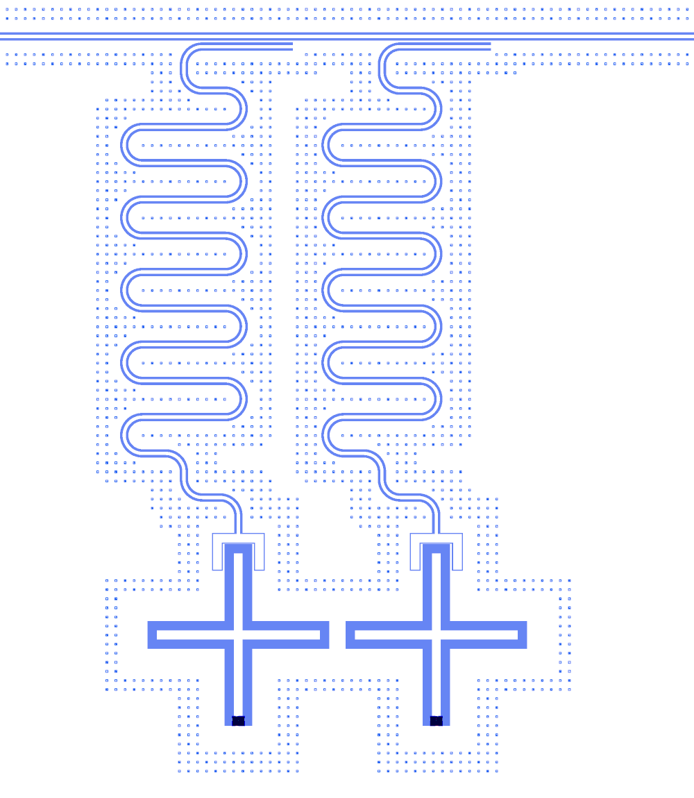
Section 4: the two qubits with their facing arms and the two meandered λ/4 readouts.
10: “I want f_q1 = X GHz”
F_Q1_WANTED = 5.45 is the input. The notebook takes the targets with your f_q1, applies the last FEM correction (from
the newest revision that has FEM results), runs the LOM loop to new knobs, rebuilds, checks the DRC and solves the new
revision with RUN_FEM. Q1’s cross moves first; outside 300 to 600 µm the junction moves instead, inside the PDK R_n
window. A frequency the window cannot reach shows up as a residual; nothing changes silently. With the kept results:
Quantity |
Target |
LOM |
Predicted |
FEM |
|---|---|---|---|---|
|
5.45 |
5.7723 |
5.4464 |
5.4546 |
|
5.65 |
5.9948 |
5.6509 |
5.6588 |
|
7 |
7.1454 |
6.9999 |
6.9907 |
|
7.3 |
7.4230 |
7.3001 |
7.2629 |
|
10 |
10.1015 |
10.0466 |
10.2866 |
The residual over tolerance is 0.92 for Q1, 1.76 for Q2, -1.85 for R1, -7.42 for R2 and 0.96 for g: Q1 and g are within tolerance, the rest are not, and the notebook says “run the feedback again (section 8)”. The cross of Q1 went from 385.97 to 371.89 µm and the strip from 50.449 to 63.991 µm.

Section 12: Q1 and its readout claw before your f_q1 change (revision 0).

Section 12: the same view after the change (a shorter cross).
11: the fab layout
export_fab writes the PDK fab layers (flat): the metal etch with the build’s cheese (3083 holes), the junction
layers, the 3/0 keep-out, the frame and markers, with rounded corners (junction fingers stay sharp). The report counts
the polygons per layer (M1 3091, M3 3087, JJ_STRAIGHT 2, JJ_BENT 2) and pdk_report lists the PDK checks (0
design warnings).
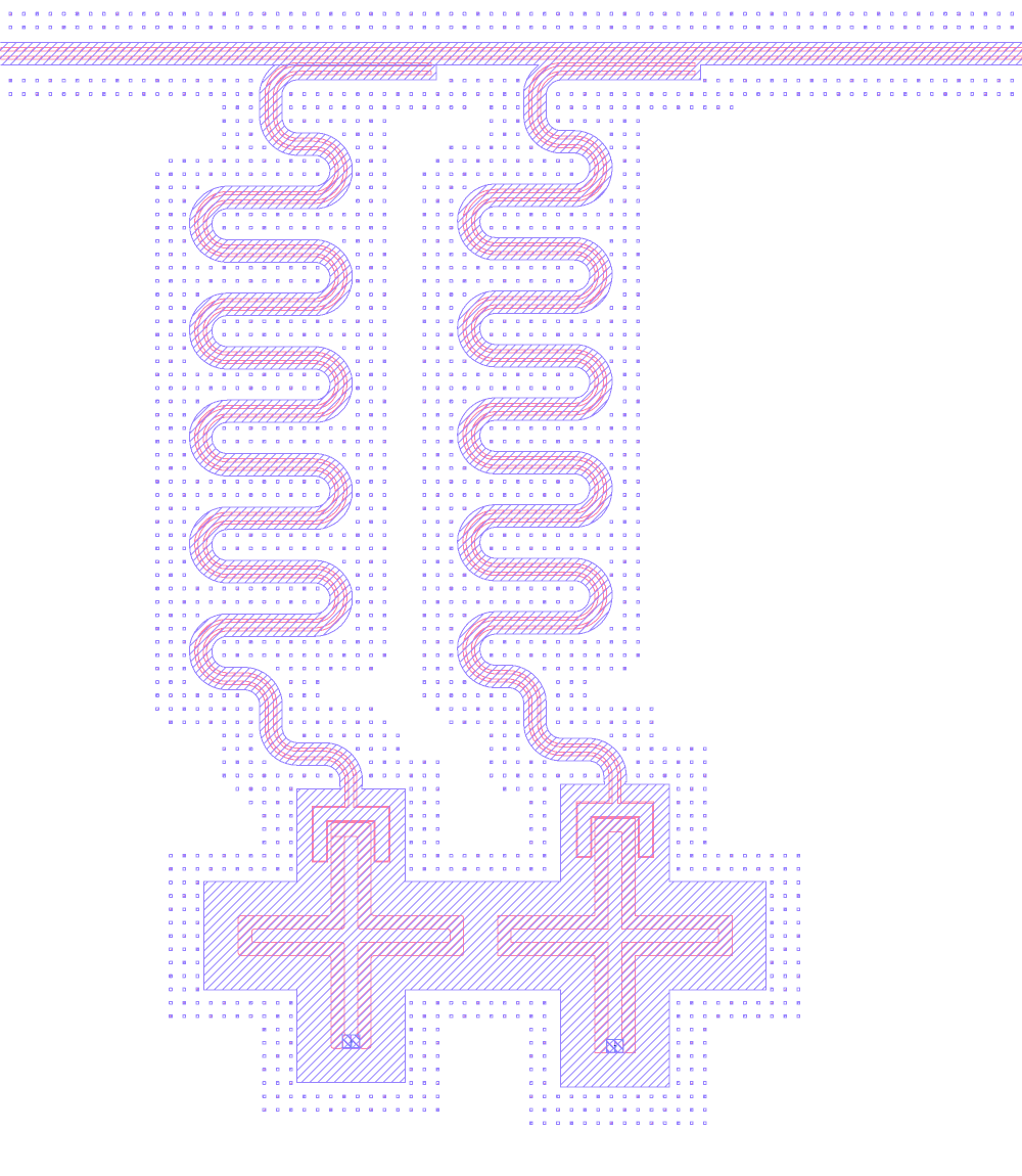
Section 11: the fab layout of the pair.
CLI equivalents from the summary cell: qcc build examples/tutorials/designs/t04_two_qubit_user.json --show,
qcc design drc ..., qcc circuit export ... and qcc circuit simulate ...,
qcc hfss render examples/tutorials/designs/t04_two_qubit.json -g PAIR -a q3d_cmatrix --solve, qcc hfss check build/jobs/<job> and qcc mask .... See Simulation and Fab.
Pitfalls
The FEM results are fast-setting runs. The eigenmode ΔF reached 2.8 to 3.2 % against 1 %. The feedback step corrects by the difference between two such runs, so its accuracy is limited by their convergence.
The kept results of revisions 1 and “user” are for the saved designs. If you change the knobs, the design hash changes and the notebook prints “solved for another revision” or no kept result; re-solve with
RUN_FEM = True.A frequency outside the PDK R_n window shows up as a residual. Look at the
residual/tolline.A LOM that is on target does not mean the FEM is. Tutorial 0 showed this on one qubit; here the FEM started 6 % low and the loop corrected most of it in one pass.
One FEM iteration (Q3D plus eigenmode) is about 25 minutes of solve time on the workstation.
The other pages are listed on the tutorials index.